Aries: An LSI Macro-Block for DSP Applications
![[PREV]](PIC/back.gif)
![[TOC]](PIC/toc.gif)
![[NEXT]](PIC/fwd.gif)
In this section, we present the overall architecture of a dedicated chip, Taurus, which is a fully pipelined real-time programmable 3x3 image filter [3,7] based on Capacitive Threshold Logic (CTL) [8]. This chip has essentially been designed to demonstrate the capabilities and possible applications of a new circuit technique (CTL) in digital signal processing. This material is presented to serve as preliminary background for the Aries architecture which will be introduced in Chapter 4.
The extensive research on CTL has resulted in a wide range of building blocks like multipliers, parity generators and population counters. CTL blocks have the advantage of realizing high fan-in building blocks with a much lesser complexity than a CMOS counterparts. As most of these blocks have costly CMOS realizations, traditional designs often tend to avoid algorithms employing functions with high fan-in. Having developed these fast and compact blocks, research intensified on the realization of complex digital systems using CTL building blocks.
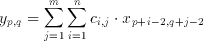
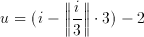
A number of applications and algorithms have been examined for their suitability to include CTL building blocks [8,9,10,11]. The time-domain two dimensional convolution (among others) proved to be suitable candidate for a CTL based application. The two dimensional convolution filter, depending on the window-or-kernel size of the filter, involves the multiplication of data values with their corresponding coefficients and the accumulation of the weighted sum of all the product terms. Thus an n x m filter needs n*m multiplications and n*m-1 additions with a total of 2*n*m-1 operations per result. These operations can be defined in mathematical notation as:
 (3.1)
(3.1)
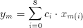
where x(p,q) is an element of the input set, y(p,q) is the filter result corresponding to the input and c(i,j) are the coefficients of the n x m window (kernel). The realization of an 3x3, (n=m=3) image filter was targeted as a demonstration of capabilities of the CTL blocks. Rewriting equation 3.1 for the given values of n and m we get
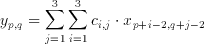 (3.2)
(3.2)
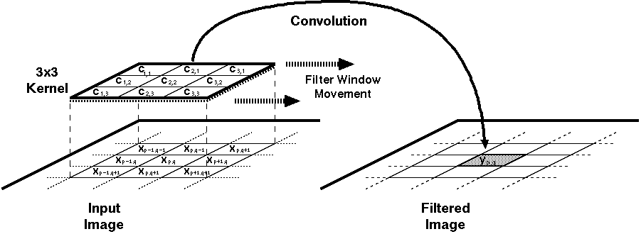 Figure 3.1: 3 x 3 convolutional filtering.
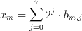
A real time implementation of this filter will need to have access to three subsequent lines (rows of pixels) of the image at any time during its operation. Three new values from each line needs to be taken at each clock cycle (Figure 3.1), thus at any given time the hardware would have access to any of these pixel values and the 2 dimensional convolution function can also be simplified into a 1-D FIR algorithm as follows:
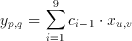 (3.3)
(3.3)
where the indexes for the 2 dimensional position of the input pixel can be calculated from the 1 dimensional variable i using modulo and remainder operations:
 (3.4)
(3.4)
and
 (3.5)
(3.5)
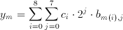
Having this conversion form i to (p,q) in mind, equation 3.3 can be written in a more simplified way such as
 (3.6)
(3.6)
A traditional high-speed implementation of this algorithm requires 9 parallel multiplier circuits to compute each product term, and an adder to calculate y(m) which increases the silicon area significantly [1].
A totally different approach to this problem can replace all multipliers with population counters. For image processing applications one may assume that x(m) is a 8 bit unsigned integer corresponding to the intensity of a pixel in the input image (Although any other value might also have been used within the algorithm). Any x(m) can be written as
 (3.7)
(3.7)
 (3.8)
(3.8)
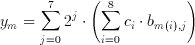
where b(m,j) element of {0,1} is the j.th bit of the m.th image pixel. Breaking down image pixels into bits leads to the definition of bitplanes which are 2 dimensional arrays that have the same dimensions as the image, but only consist of the j.th bit of the image pixel values (see Figure 3.2). Substituting this representation of a binary number in Equation 3.6 we get:
 (3.9)
(3.9)
Using the associative property, we can further modify this equation into
 (3.10)
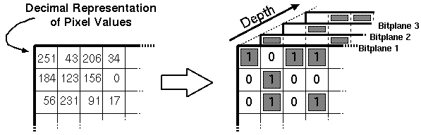 Figure 3.2:Bitplane representation of a binary coded image.
This re-arrangement is very important in understanding the operation principle of the Taurus architecture. The inner parenthesis which involves a multiplication is a special multiplication operation as one of the operands has only two possible values (b(m,j) element of {0,1}). Therefore, the result of the multiplication can be expressed as:
 (3.11)
 (3.12)
The inner sum therefore, is only a conditional sum of the coefficients. Taurus uses a CTL based counter to generate this sum. An input switch matrix provides a programmable switch for each of the coefficients. If b(m(i),j)=1, c(i) number of inputs of a counter are made active. The counter simply counts the number of logic "1"s on its input which is the sum of all coefficients which have a non-zero corresponding bit on the bitplane. Once this sum is generated for each bitplane of the image, the result is obtained by weighting and adding these sums. The j.th sum has a weight of 2^j, but this weighting is relatively easy to implement with by the means of a simple j bit shift left operation. In fact, the shifting operation can easily be implemented within the adder with no extra cost at all.
![[TOP]](PIC/up.gif)
Threshold Logic (TL) emerged in early 1960's as a unified theory of logic gates, which includes conventional switching logic as a subset. The formal TL gate can perform not only and/or primitives but any linearly separable boolean function [12]. But despite the theoretically obvious merits, until recently TL has never had a significant impact in practice, due to the limited success achieved in developing a suitable TL gate on silicon.
The similarities between the functionality of a TL gate and the hard limiting neuron structures used in artificial neural networks, has led to the development of Capacitive Threshold Logic (CTL) gates [8].
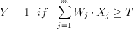
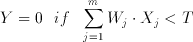
The CTL circuit technique offers a successfull implementation of threshold functions using conventional CMOS processes. A threshold gate is defined as an m input gate where the output Y is defined as follows:
 (3.13)
 (3.14)
where X(j) is the j.th binary input with a corresponding weight of W(j). A basic CTL gate of m inputs, as shown in Figure 3.3, comprises a row of weight-implementing capacitors C(i) and a chain of inverters which functions as a voltage comparator.
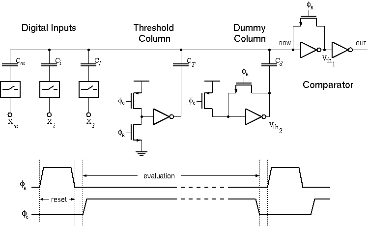 Figure 3.3:Basic circuit diagram of a Capacitive Threshold Logic (CTL) gate.
The CTL gate operates in a two phase non-overlapping clock consisting of a reset phase defined by the clock phi-R and an evaluation phase defined by phi-e. During the reset phase, the row voltage Vrow is reset to the threshold voltage of the first inverter Vth1 . The bottom plates of all input capacitors are forced to ground potential while all the threshold capacitors have their bottom plates connected to VDD. The total charge accumulated in the row during reset can be calculated as follows:
 (3.15)
where Vth1 is the inversion (logic) threshold voltage of the first inverter within the comparator and Vth2 is the inversion (logic) threshold voltage of the inverter in the dummy column. In the evaluation phase all binary inputs are forced onto the m input columns while the threshold capacitors are connected to ground potential. The amount of charge in the row, for a given set of inputs, can be calculated as follows:
 (3.16)
Since the row charge is retained (charge conservation) during both operational phases, the row voltage perturbation during the evaluation phase becomes:
 (3.17)
The row perturbation is equal to the difference between row voltage in reset and evaluation phases.
 (3.18)
Substituting this in Equation 3.17 yields
 (3.19)
Notice that the first inverter of the comparator circuit is biased exactly at inversion threshold Vth1, which is also the operating point with the highest gain, at the beginning of the evaluation phase. If the voltage perturbation Delta Vrow is positive, the first inverter output will tend to drop to logic "0" and the second inverter will switch to logic "1". If the voltage perturbation Delta Vrow is negative, the opposite will happen.
 (3.20)
 (3.21)
It can be seen that Equations 3.20 and 3.21 correspond to the basic threshold gate Equations given in 3.13 and 3.14.
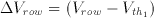
The CTL-based parallel counter (i.e. population counter) circuit constitutes the heart of the Taurus architecture [10]. A parallel counter is a multi-input, multi-output combinational logic circuits which determine the number of logic "1"s in their input vectors and generate a binary encoded output vector which corresponds to this number.
A traditional CMOS realization of a parallel counter involves a number of full adders (FA's) arranged in a tree like structure (See Figure 3.4). Swartzlander [13] reports the number of FA's for an m-input population counter as
 (3.22)
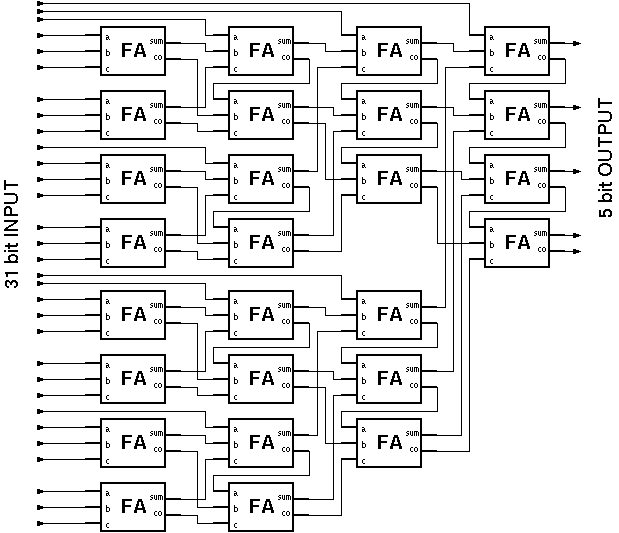 Figure 3.4: Full Adder (FA)-based realization of a (31:5) parallel counter.
Different threshold logic realizations of the population counter exists in the literature [14,15,16]. The CTL realization of the parallel counter used in this work is based on the two level Minnick counter (Figure 3.5).
 Figure 3.5: Threshold Logic realization of a Minnick Type (31:5) parallel counter .
The basic architecture of the Taurus comprises of the basic building blocks given in Figure 3.6:
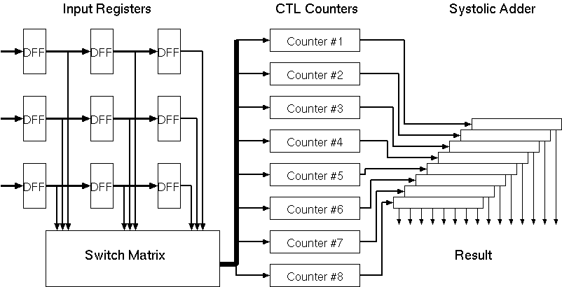 Figure 3.6: General Architecture of the Taurus image filter chip.
Input registers:
At any given time the Taurus architecture needs access
to a 3x3 snapshot of the image. Three rows of shift registers with
a depth of three are used to store this snapshot.
Switch matrix:
Each input bit within the input data has a corresponding
weight. For a logic "1" bit, this weight is applied to the inputs
of the counters. The switch matrix is used to store the filter weights.
Each element within the switch matrix is trigerred by a different
bit of the input image and can activate a programmable number of inputs
of counters.
The CTL counters:
For an 8-bit image, eight independent counters are
used to accumulate the weights of corresponding bits. The switch matrix
activates a number of inputs on each counter depending on the value
of the corresponding bit. The total number of active inputs is accumulated
by the CTL counter blocks.
Systolic adder tree:
The output of the CTL counters corresponds to
a partial sum of one bitplane of the image. All eight partial sums
need to be added to get the result. Since each bitplane has a different
weight, they can not be added directly. The systolic adder tree shifts
(and thereby multiplies) the partial results according to their rank
and accumulates the final result.
This basic architecture has been refined to achieve higher performance.
Figure 3.7 shows the final detailed block diagram of the Taurus architecture with all these improvements and the pipeline registers.
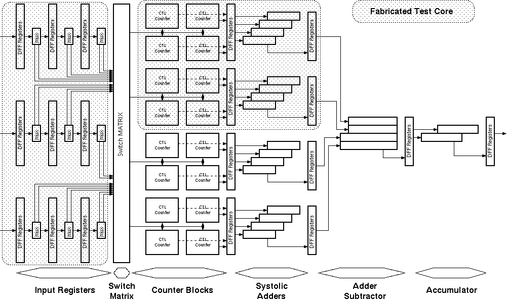 Figure 3.7: Detailed block diagram of the Taurus architecture.
To evaluate the performance of the proposed architecture a test chip has been designed and developed (See Figure 3.8) using conventional 1.2um double-poly double-metal CMOS technology. The chip contains a fixed weight version of the processing core which realizes a (3 x 3) smoothing function. The switch matrix array, which is used to facilitate coefficient programming, has been omitted to simplify testing. The realized test structure contains three eight-bit-wide and three-bit-deep input shift registers which facilitate simultaneous input of three eight-bit pixels during each cycle, the corresponding bitplane multiplexers, eight CTL-based parallel (30,5) counters, and two systolic adder arrays. edge triggered dynamic CMOS register cells were used for all pipeline registers. the parallel counters and the adder arrays each form separate pipeline stages in order to reduce the stage delays (These blocks can be seen in Figure 3.7 as shaded blocks).
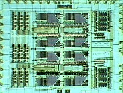 Figure 3.8: Microphotograph of the fabricated Taurus core test chip.
Extensive post-layout simulations have shown that the signal propagation delay associated with the CTL based parallel counters is about 10 ns, whereas the overall delay of the CMOS adder array stage is well below 10 ns, using a supply voltage of 5 V. Thus, the maximum clock frequency can be as high as 100 MHz, allowing real-time processing of high-resolution (1024 x 1024) pixel images at a rate of 50 frames per second.
The core area of the implemented test chip 1.8 mm x 1.5 mm compares very favourably with other image filters using a similar fabrication technology. About 60% of the active area of the chip is occupied by the CTL counters and their input and output registers, while the systolic adder arrays occupy around 15% of the total area.
Although tests were hampered by different reasons, the calculation time for a single vector was measured to be around 7.9 ns [7] which is well under the designed 10 ns.
A number of problems both in the design and the implementation of the algorithm have been detected after carefull analysis of the Taurus design:
A number of solutions to address the above mentioned problems have been evaluated and as a result of this research Aries was developed. In Aries the basic idea of computing a convolution without using conventional multiplier cells, in breaking up the input (image) data to bitplanes remained the same, but RAM blocks were used to calculate bitplane results instead of CTL blocks.
 KGF
KGF