Aries: An LSI Macro-Block for DSP Applications
![[PREV]](PIC/back.gif)
![[TOC]](PIC/toc.gif)
![[NEXT]](PIC/fwd.gif)
![[PREV]](PIC/back.gif)
![[TOC]](PIC/toc.gif)
![[NEXT]](PIC/fwd.gif)
Two main problems in the design of Taurus became primary considerations in the design of Aries: scalability and programmable coefficients with a higher dynamic range.
Although many applications could make use of a 3x3 image filter, a scalable building block is much more desirable than a block with a fixed kernel size. Any kernel with size M x N can be realized by accumulating the results of a number of kernels with smaller sizes m x n where M >= m and N >= n. It can be shown that the number of such m x n kernels needed is:
 (4.1)
(4.1)
Scaling of the filter kernel along the Y axis does not impose extra restrictions on the design but in order to scale along the X axis, the block must be able to provide the outputs of the internal shift registers to the next stage. If this is not the case, the same delay must be provided externally to the block. This would result in a non uniform structure as the first block would need no delay elements, the second would need m delay elements, the third 2m and so on. The last problem rises in the addition of all the block results. As the complexity of the addition increases with the number of blocks included, it is not convenient to leave this task out of the block. The block needs to provide some sort of support for the addition of a number of results.
Integer coefficients of up to 15 might be reasonable (though more would be desirable) for a 3x3 filter. But filters with a larger kernel usually need a higher coefficient range. A possible solution is to scale all coefficients of one block with a fixed number, thus changing the range of the coefficients locally. This solution might be applicable for a number of applications but is not sufficient enough for a complete solution.
Increasing the coefficient range within the Taurus architecture is only possible by adding more parallel counter blocks. The increase in the number of counters would also complicate the internal routing to an almost unmanageable level, while further complicating the later adder stages. An algorithmic improvement is inevitable for a significantly higher coefficient dynamic range.
Aries is designed to be a building block for convolutional filters and the main design issue is on scalability. Therefore the design has to:
As scaling in the Y dimension did not have any extra complexity penalty a one dimensional structure was used for Aries. Almost all filters have odd sized dimensions and therefore an even sized block would not be very practical. 3x1 proved to be too small to justify the overhead involved in the architecture and blocks larger than 5x1 would have too much redundancy in them for small to medium sized filters (which usually are 3x3 or 5x5 . As a result, Aries was designed to provide the functionality of a 5x1 one dimensional convolution filter that could be expanded to realize 1D and 2D convolutional filters of any complexity.
![[TOC]](PIC/toc.gif)
![[TOP]](PIC/up.gif)
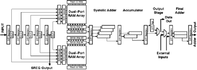
![[ZOOM]](PIC/mag.gif) Figure 4.1: General block diagram of the Aries architecture.
Figure 4.1: General block diagram of the Aries architecture.
The basic DSP algorithms implemented by the Taurus and Aries architectures are very similar. The general block diagram of the Aries architecture is shown in figure 4.1. Aries has a 5 level shift register on its input (as opposed to 3 in Taurus) to have simultaneous access to all the data elements. The main difference between the two designs lies in the calculation of the conditional sums of the coefficients on a bit plane. The CTL-based parallel counters in the Taurus architecture are replaced by RAM blocks in the Aries architecture . Once the problem of calculating the result
 (4.2)
(4.2)
has been reduced to adding the conditional sums of all bitplanes:,
 (4.3)
(4.3)
it was shown that the inner sum could be calculated by simply adding or neglecting the associated coefficient c(i) depending on the value of b(m). As the block only needs five values of the input source, this sum is a linear combination 5 coefficients. Different algorithms can be devised to calculate the sum of coefficients of any length, but as long as the coefficients do not change there will be only 2^5=32 different results depending on the 5-bit value of the input pattern. If a 32-word memory (note that in the case of fixed coefficients, a simple ROM can be used for this purpose) is used to store all the possible results, this sum can be calculated independently of the coefficient representation. To provide programmability a RAM structure was used in Aries. As the delay of reading data from RAM is independent of the word size any length of coefficients can be used. Table 4.1 lists all possible conditional sums depending on the input data.
Table 4.1:All possible conditional sums as a function of input data.
Data        Sum           Data          Sum
-----------------------------------------------------
00000       0             10000         c5
00001       c1            10001         c5+c1
00010       c2            10010         c5+c2
00011       c2+c1         10011         c5+c2+c1
00100       c3            10100         c5+c3
00101       c3+c1         10101         c5+c3+c1
00110       c3+c2         10110         c5+c3+c2
00111       c3+c2+c1      10111         c5+c3+c2+c1
01000       c4            11000         c5+c4
01001       c4+c1         11001         c5+c4+c1
01010       c4+c2         11010         c5+c4+c2
01011       c4+c2+c1      11011         c5+c4+c2+c1
01100       c4+c3         11100         c5+c4+c3
01101       c4+c3+c1      11101         c5+c4+c3+c1
01110       c4+c3+c2      11110         c5+c4+c3+c2
01111       c4+c3+c2+c1   11111         c5+c4+c3+c2+c1
Aries also uses the time multiplexing scheme to operate only on 4 bit planes at any given time. As each bitplane may have different data bits to be processed simultaneously, four different RAM structures have to be used. But since all of the RAM's would hold exactly the same information, it is not necessary to have four completely different RAM blocks. Figure 4.2 shows three existing alternatives:
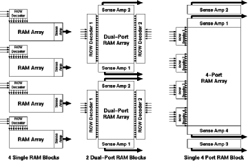
![[ZOOM]](PIC/mag.gif) Figure 4.2:Three alternative designs for the RAM blocks which are to be used
to store the conditional sums.
Figure 4.2:Three alternative designs for the RAM blocks which are to be used
to store the conditional sums.
Of the different RAM realizations, the Static RAM (SRAM) realization was used in the design of the Aries architecture, because it is easier to design and more robust than the other alternatives. The double dual-port alternative was used in the design, since the basic cell for a dual-port RAM cell was not much more complex than the single-port RAM cell, keeping the overall size of the RAM block compact. The quad-port RAM would have benefited from maximum resource sharing; but the basic cell proved to be too complex, as the extra routing overhead nearly cancels out all the area gained by the single RAM array. The dual port architecture had another advantage: As the RAM is laid out in a column, a totally symmetric structure could be used for both ends of the column (Although this advantage was later given up in favour of shorter signal routing paths).
The output of the RAM's is later shifted and added in a systolic adder that is similar to the one used in Taurus. There is an interesting speed/accuracy trade off parameter that can be adjusted within these two blocks. As mentioned earlier, the speed of RAM is independent of the word width, whereas the speed of the systolic adder heavily depends on the word width of its operands. As both of these blocks are in different pipeline stages, they can be optimized to match each other, minimizing the pipeline redundancy.
The results from the upper and lower parts of the blocks are merged in a separate accumulating adder which again has the same structure as the accumulator that was used in Taurus. The result of this operation is actually the result of the operation. This value will correspond to the new value of data, but it has to be reformatted to the same range as the input: an 8-bit unsigned integer value. This involves some sort of truncation and rounding which heavily depends on the coefficients and the input data ranges.
At this point the data is ready for output. The block includes an additional adder stage that can be configured to be part of an adder chain to add the results of all blocks in the filter.
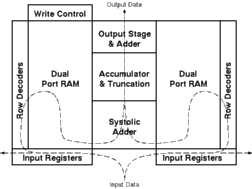
![[ZOOM]](PIC/mag.gif) Figure 4.3: General floorplan of the Aries DSP engine.
Figure 4.3: General floorplan of the Aries DSP engine.
Figure 4.3 shows the basic floorplan of the Aries DSP engine. The dashed line in the figure shows the flow of data within the blocks. Rough pre-design estimations suggested the size of the final layout to be between 2mm^2 and 4mm^2 using the 0.8um double-metal CMOS technology of the Austria Micro Systems (AMS). The extremely compact size and the high-flexibility of the Aries architecture makes it possible to construct even the most demanding and complex image filters within a single chip.
Aries consists of several independent blocks (see Figure 4.1):
![[TOC]](PIC/toc.gif)
![[TOP]](PIC/up.gif)
The Aries architecture computes the weighted sum of five consecutive signal values. A simple structure consisting of five shift registers is used to store these consecutive data. The 8-bit input data is sampled at the rising edge of the first clock cycle by the first register. The output of the first register is connected to a second one, and at the second rising edge the data is sampled by the second stage registers while at the same time the first stage registers sample a new data. After the first five clock cycles, the block has access to five consecutive data values and can calculate a weighted sum for these values. At each new clock cycle a new value enters the shift registers and the last value is pushed out of the block.
The Aries architecture is designed as a pipeline structure to speed-up the operation. The signal flow is broken down into several sub-blocks separated by registers. At each clock cycle, the output of each block is sampled by a pipeline register. At the same time the result of the previous block is sampled by another register block and is made available as an input to the first block. Each block has a fixed time determined by the clock rate of the pipeline registers to compute the result.
Instead of calculating all results for 8-bits in n clock cycles, the architecture consists of inner blocks that operate on 4-bit data and produce a new result in n/2 clock cycles. The outputs of the shift registers have a simple multiplexer structure that selects the lower order 4-bits while the clock signal is high and selects the higher order 4-bits when the clock signal is low. These 4-bit partial-data is processed with a faster clock of 2f frequency within the inner blocks and the partial results are joined in the accumulator block. The general pipeline structure of the Aries architecture is shown in Figure 4.4.
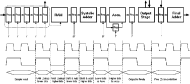
![[ZOOM]](PIC/mag.gif) Figure 4.4: Timing diagram of the pipeline.
Figure 4.4: Timing diagram of the pipeline.
The design of the pipeline registers is a very important phase of any pipeline based design. Generally, a large number of registers have to be used. As an example, Aries uses 170 pipeline registers throughout the design. Table 4.2 lists the distribution of registers for various blocks. As mentioned earlier, each block is allotted a certain time to finish the calculations before the output is sampled by the output register. For extremely fast pipeline stages the sampling speed of the register itself is a critical factor. In Aries the inner blocks (which operate on a faster clock) are designed to operate in a 10 ns pipeline. This 10 ns includes the calculation delay of the block plus the sampling time of the register. Therefore, it is highly desirable to have a register that is extremely fast (<1 ns).
Table 4.2:Number of registers used throughout Aries.
Name                       Number       Clock

Input Shift Registers     5*8 = 40        f
RAM outputs              4*10 = 40        2f
Sys. Adder outputs              13        2f
Accumulator                     13        f'
Accumulator Outputs             16        f
Output Stage                    16        f
Final Adder              2*16 = 32        f
----------------------------------------------
TOTAL                          170
Two basic circuits are widely used to realize pipeline registers. The most common solution is to use a latch. A simple and efficient latch can be realized with as few as 4 transistors. The main problem is that the circuit requires two complementary clocks. The second alternative is to use a D-type flip-flop (DFF) which is edge trigerred (contrary to the latch which is level sensitive). DFF's are usually preferred for their relative robustness over simple latches in many applications, even though the circuit complexity of a typical DFF is usually twice of that of a simple latch, due to the Master-Slave configuration. All registers within Aries are realized as modified Yuan-Svensson D-type flip-flop [18], whose circuit schematic is given in Figure 4.5.
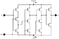
![[ZOOM]](PIC/mag.gif) Figure 4.5: Schematic of the Yuan-Svensson D-type flip-flop.
Figure 4.5: Schematic of the Yuan-Svensson D-type flip-flop.
The Yuan-Svensson Flip-Flop is one of the fastest and most compact D-type flip-flop realization available. The circuit is based on the True Single Phase Clock (TSPC) principle and requires a single data and clock signal for operation. Its high operation speed and low transistor count make it an interesting alternative for traditional latch architectures. Figure 4.6 shows a simulation result of the Yuan-Svensson D-type flip-flop (all nMOS transistors W=2um, and all pMOS transistors W=5.6um. The simulation shows that even without aggressive transistor sizing, the Yuan-Svensson D-type flip-flop is able operate much faster than 1 ns.
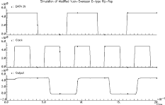
![[ZOOM]](PIC/mag.gif) Figure 4.6: Simulation result of the Yuan-Svensson D-type flip-flop.
Figure 4.6: Simulation result of the Yuan-Svensson D-type flip-flop.
The 8-bit outputs of the shift registers are pairwise fed into a multiplexer. This multiplexer selects the lower order 4-bits for the high value of the clock signal and the higher order 4-bits for the low value of the clock. The output of each multiplexer in a shift register block drives a separate address line of the RAM. Combining the outputs of multiplexers in five rows, four different RAM address lines of five bits each aregenerated. The simple 2:1 multiplexer circuit would be sufficient for read only operation. For write operations the address lines of the RAM blocks must be controlled separately. A third mode where the address lines are tied to an external data bus is used to create a simple interface to the outside world. Figure 4.7 shows the block schematic of the input stage.
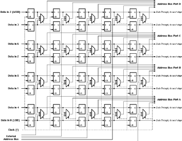
![[ZOOM]](PIC/mag.gif) Figure 4.7: Block mode schematic of the input registers.
Figure 4.7: Block mode schematic of the input registers.
The shift registers are laid out in two separate blocks in order to drive the address decoders of the Dual-Port RAM structure. Figure 4.8 shows the layout of one of the input register blocks. The layout consists of two separate paths, each having 2 x 5 Yuan-Svensson D-type flip-flops, and each register pair is followed by a three input multiplexer. The external address lines are shared by both paths, and they are located in the middle of the bus seen to the center of the cell. All clock and power signals are routed horizontally over the cells. The layout occupies an area of 320um x 140um.
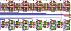
![[ZOOM]](PIC/mag.gif) Figure 4.8: The layout of the input shift registers.
Figure 4.8: The layout of the input shift registers.
![[PREV]](PIC/back.gif)
![[TOC]](PIC/toc.gif)
![[TOP]](PIC/up.gif)
![[NEXT]](PIC/fwd.gif)
 KGF
KGF