Aries: An LSI Macro-Block for DSP Applications
![[PREV]](PIC/back.gif)
![[TOC]](PIC/toc.gif)
![[NEXT]](PIC/fwd.gif)
The main algorithm implemented by the Aries architecture is based on the fact that for m inputs, (regardless of the complexity of the data and coefficients involved) there can be only 2^m different results, all of which can be stored within a processing pipeline to reduce computational complexity. This is only possible if:
A number of factors need to be evaluated to see if the above mentioned requirements can be met. It is clear that the efficiency heavily depends on the number m, the data storage method and the width of coefficients as well as width of data involved in the convolution.
Generally speaking, for a convolution over m input cells with a data width of b bits with a set of kernel coefficients to get a result k bits wide, the total amount of required storage can be expressed as
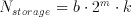 (5.1)
(5.1)
It must be noted that the storage for each bitplane will be identical, resulting in
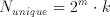 (5.2)
(5.2)
unique storage cells. These two expressions clearly show that regardless of the storage method a memory based solution is not very efficient for large values of m. Yet for a simple building block, large values of m are not needed. Even values of m are also not very practical as most convolutions used in DSP algorithms need the data point plus an equal number of neighbours, commonly resulting in a matrix of odd dimensions. Table 5.1 compares the amount of memory to the number of multiplications (assuming k=10) for selected values of m.
Table 5.1:Number of operations.
m            N-unique    8x8 Multiplications

3               80                 3
5              320                 5
7             1280                 7
In this work, m=5 was found as a more reasonable candidate as it has a relatively small memory requirement which is large enough to justify the peripherals associated with the storage elements. At first sight, the amount of computational complexity that the storage replaces may not seem significant. Multiplication is one of the most demanding and area consuming operations in the digital domain. Aries, as an example, uses m=5 and the storage elements can deliver the result of 5 multiplications in 10 ns, in a technology where a well designed Full Adder has a delay of about 1 ns. The same performance can only be achieved by the utilization of at least two (or more) multiplier blocks. Moreover the delay of the storage elements is independent of the coefficient dynamics, that is to say a result of any bit length will be delivered at the same rate as the 10-bit result. This allows for optimization in the bit-length, by which the delays of all pipeline stages can be carefully balanced to match the speed of storage elements, as increasing word lengths accounts for increasing processing in the subsequent combinational adder stages.
![[TOP]](PIC/up.gif)
It is a known fact that the flagship of integrated circuits development is the realization Random Access Memory devices. Current technology is often referred in terms of storage elements per chip (such as 1 G-bit technology). Yet much of these advanced technologies are not available for common digital designs and large on-chip memories are not desirable, mainly because of their area requirements.
For small and medium scale storage within the constraints of conventional digital VLSI technology two practical solutions exist:
The most important advantage of the register array, which basically consists of an array of D-type flip-flops, is that the designer can safely use standart cell elements to generate the register array, completely avoiding the time-consuming full custom design effort. Most of the modern synthesis tools support these arrays and many contemporary designs include relatively large amounts of such structures. But the register array design also has several disadvantages:
 Figure 5.1: 2 x 2 SRAM array compared to 4 x 1 DFF array.
Figure 5.1 clearly shows the difference in silicon area. Even without any associated connections and peripherals, the full custom realization of a 2x2 Static-RAM ( ~1000um^2) occupies less than one sixth of the area of the registers (~6500um^2).
Although the advantages of using a RAM block is clear, it requires much more design effort than the standart cell based solution. Some semiconductor foundries have tools to automatically generate RAM blocks, while some others have services for commercial products (in which practically the foundry employs a RAM design engineer). In the case of Aries, the chosen semiconductor foundry Austria Micro Systems (AMS) did not have a RAM generator, so the RAM cells had to be designed in full custom.
Although inherently Dynamic RAM (DRAM) circuits have a much higher density, their design is much more complicated (state of the art DRAM designs rely on a broad range of technology enhancements which are not common in normal digital CMOS technologies), requires more sophisticated clocking and is usually slower than Static RAM (SRAM) circuits.
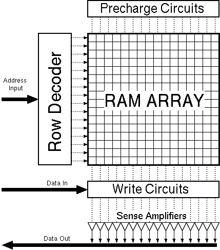 Figure 5.2:General SRAM structure.
A generic SRAM carray and its peripheral circuitry are shown in Figure 5.2. The SRAM array consists of a dense two-dimensional arrangement of the actual storage elements. For small memories it is possible to store one word of data in a row (for larger memories one row holds several words of data). All cells in one column share the same input signals (called the bitlines). Prior to read or write operations, the bitlines are charged to a known value by the pre-charge circuits. The row decoders are used to select one row in the array. The storage elements in the row are connected to the common bitlines and either the value within the cell is sensed (read) by sense-amplifiers or is overwritten by write circuits depending on the mode of operation. For large memories, an additional column decoder is used to select the desired word within a row.
A simple CMOS-SRAM cell consists of two cross coupled inverters and two access transistors connecting these two inverters to complementary bitlines.
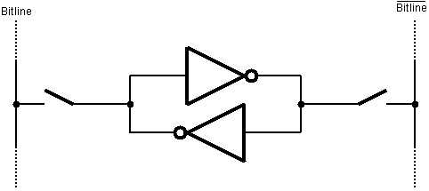 Figure 5.3: Basic SRAM cell.
The two switches in 5.3 are simple nMOS pass-transistors. A so called wordline controls these pass-transistors. As long as the pass transistors are turned off, the cell retainsone of its two possible steady state.
A read operation from this cell is performed by pre-charging the bitlines to a known value (e.g. VDD) and enabling the wordline. As during any read operation only one row can be active (the row decoder guarantees this), each column (bitline) can be modelled by a capacitor representing all the parasitic capacitance of the bitline and the input capacitance of all the access transistors. Figure 5.4 shows the pre-charge circuitry and the simple SRAM cell itself, together with the column capacitances.
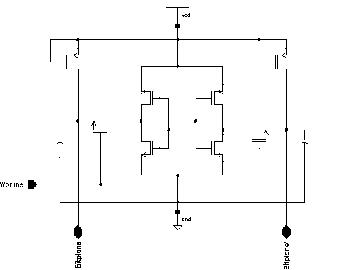 Figure 5.4: Equivalent SRAM cell during Read and Write operations.
Depending on the content (i.e., the state) of the cell, one of the bitlines will be pulled down by the nMOS transistor of the inverter with the logic "0" state, while the other bitline will remain at VDD.
Figure 5.5 shows the simulation results of two consecutive read operations. The nMOS transistors of the simulated RAM cell have dimensions of W=3um and L=0.8um while the pMOS transistors and the access transistors are minimum width transistors, having dimensions of W=2um and L=0.8um. The parasitic bitline capacitance is modeled to be 1pF. The first Read Cycle starts at 160 ns with the activation of the wordline. The stored information is a logic "1", bitline rises to VDD while bitline' is pulled down by the second inverter. Notice that the bitline is not pulled down completely (in fact it only reaches 4 Volts) but that is enough for the sense amplifier to operate correctly. The second read operation starts at 180 ns with the activation of another wordline (not shown, which in fact is just the inverted first wordline). This time the stored information is a logic "0" and the switching of the bitlines can be seen clearly.
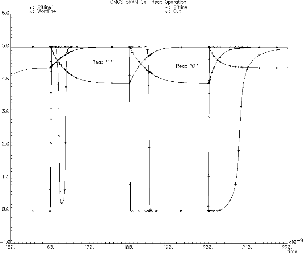 Figure 5.5: Simulated SRAM read operation.
A write operation is pretty similar in nature to the read operation. Again the cell is accessed with enabling the wordline, but this time the bitlines are driven to a known state by the write circuitry. This write circuitry is designed to have a stronger current driving capability than the pre-charge and storage cell circuitry, and as a result the bitlines are driven beyond the inversion thresholds of the inverters within the SRAM cell.
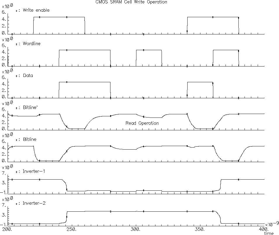 Figure 5.6: CMOS SRAM Write operation.
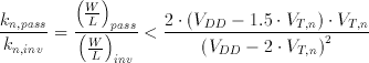
The plot in Figure 5.6 is a snapshot of a simulation used to verify the functionality of the RAM design. The first three strips are the control signals. Write enable signal activates the write mode, Wordline selects the rows to be accessed and the Data is the value to be written to the selected cell. The voltages of the bitplanes is plotted next followed by the voltages within the SRAM cell. (the inputs of the two inverters). The simulation snapshot displays consecutive write and read cycles. The first write cycle starts at 220 ns. A logic "0" is written to a cell within the column which is not the cell that we are concentrating. At 240 ns. a logic "1" is written into the cell. The Wordline goes high indicating a write to the cell we are observing. Notice the bitline swing for the write operation. Also the last two strips clearly show the switching inverters. A new value has been written. There is a read cycle starting at 280 ns. At 300 ns our cell is accessed for a read operation. Notice the relatively low bitline swing and the perturbation on the inverter. It is clear that a perturbation as high as the threshold voltage of the nMOS transistor may cause the inverter switch state and destroy the content of the cell. Kang and Leblebici [19] give a conservative analytical expression for the sizing of access and pass transistors to prevent overwrite during read.
 (5.3)
(5.3)
Substituting the values for the AMS 0.8um process VDD=5V and Vt,n=0.75V we get.
 (5.4)
(5.4)
The simulation shows a second write operation starting at 340 ns. At 360 ns logic "1" is written to the cell activated by the Wordline .
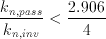
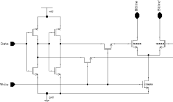
To achieve a higher RAM density, Aries uses dual port RAM cells. As each port must be able to access the cell independent of each other the basic access lines Bitline, Bitline' and Wordline need to be duplicated. Two more pass transistors are added to control access of the second port (See Figure 5.7).
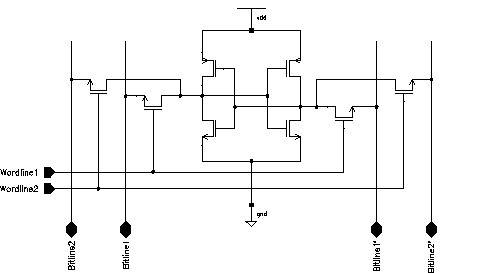 Figure 5.7: Dual-Port CMOS SRAM cell schematic.
An efficient layout for the basic cell is the key point of any dense RAM circuit layout. There are a few important factors to consider when designing a custom cell like this:
 Figure 5.8: Layout of the optimized Dual-Port CMOS SRAM cell.
Figure 5.8 gives the basic Dual-Port CMOS SRAM cell used within Aries. The basic cell measures 30.2um x 19.2um.
A very simple pre-charge circuit is used for the realization of the RAM. Unlike many SRAM designs, the SRAM in Aries does not use clocked pre-charge circuits. The RAM is targeted to operate at clock speeds of up to 100 MHz. A clocked pre-charge circuit would have needed a very accurate and complicated clock timing. The schematic of the static pre-charge circuit structure can be seen in Figure 5.9
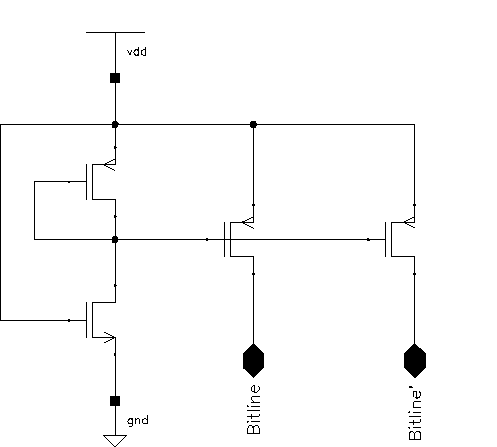 Figure 5.9: Pre-charge circuit schematic.
The pMOS transistors driving the bitlines have width of 6um , all the other transistors have dimensions of 2um. While providing a very simple column pre-charge mechanism, this structure also has some drawbacks:
The most important is that as there is a constant pre-charge voltage in the bitline, any effort to pull the bitline down must fight against this pre-charge circuit. One possible remedy would be to use minimum-size pMOS transistors in the pre-charge, but this is not feasible as a fast recovery is required to pull the bitlines from their low states to their high states. A weak pull-up would result in a slower response time in read access. On the other hand, the write operation needs to pull down the bitline even further, in order to be able to switch the internal inverters. A relatively strong write circuit easily accomplishes this task. This in turn has another negative effect. After any write operation one of the bitlines is pulled down to a relatively low voltage level. Thus, a subsequent read operation may under certain circumstances overwrite the content of the cell. Fortunately, this is not a major issue, since write operations are only required to update the weights; therefore, the write timing is not critical. In Aries, a write operation must be followed by an idle state (to help recover the bitlines) prior to a read operation. This restriction does hardly effect the operation of the circuit.
The main issue in the RAM design for Aries was the speed of read operation. The sense amplifier is the most important block that dictates the speed of read operations. The sense amplifier was developed by B. Aksoy [20]. A number of different architectures were evaluated. Finally, a two stage amplifier with a cross-coupled pMOS amplifier as the first stage and a conventional differential amplifier as the second stage was found to give the best performance. Figure 5.10 shows the schematic and the transistor sizing of the sense-amplifier circuit. Detailed evaluation and simulation results of this two-stage sense amplifier can be found in [20].
 Figure 5.10: Schematic of the Sense Amplifier.
The write circuit is a simple differential stage that is driven to saturation by Data and Data'. Two pass transistors and the current source for the differential amplifier is controlled by the Write signal. Figure 5.11 shows the schematic of the write circuit together with the sizing of non minimal transistors.
![[ZOOM]](PIC/mag.gif) Figure 5.11: Schematic of the Write circuitry.
Figure 5.11: Schematic of the Write circuitry.
A typical RAM circuit consists of an array of RAM cells that are arranged in rows and columns. The RAM can be laid out so that each row holds exactly one word of data, which for most RAM designs would generate blocks with dramatic aspect ratios that are totally unacceptable for efficient design both for their awkward geometry and the parasitics associated with especially the very long bitlines, not to mention the complicated decoder structure. For these reasons, RAM's are designed to contain more than one words in a row, with a two stage decoding process: First the row decoder selects the row of interest and than column decoders chose the required word from the selected row. Aries however required, only 32 different values for 8-16 bit data words (the exact word length was not chosen to be 10 at the beginning of the design). It was therefore possible to make an array without column decoders. The RAM array used, has an aspect ratio of 2:1 which is totally acceptable.
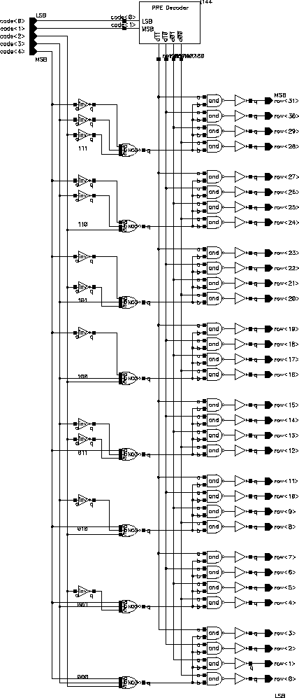 Figure 5.12: Row decoder schematic.
Five address lines are necessary to decode 32 individual rows. For the design of Aries a two stage decoding structure was used. Figure 5.12 illustrates the decoding circuitry. The box on the top is the first stage decoder (pre-decoder). Please note that the block in the figure is not logic optimized and contains a number of redundant blocks. The block diagram represents the actual logic elements realized on the layout (the AND gate as an example is realized by a combination of NAND and NOT). The local inverters on the eight blocks are used to generate the complementary signals where needed and thereby reduce the number of vertical wires in the decoder.
There are two problems associated with writing to the RAM blocks:
Both of these problems can be addressed with relatively low design effort. For the first problem a very simple state machine as shown in Figure 5.13 can be used to generate the idle times. The circuit in the Figure 5.13 generates synchronous read and write signals depending on the state of "en".
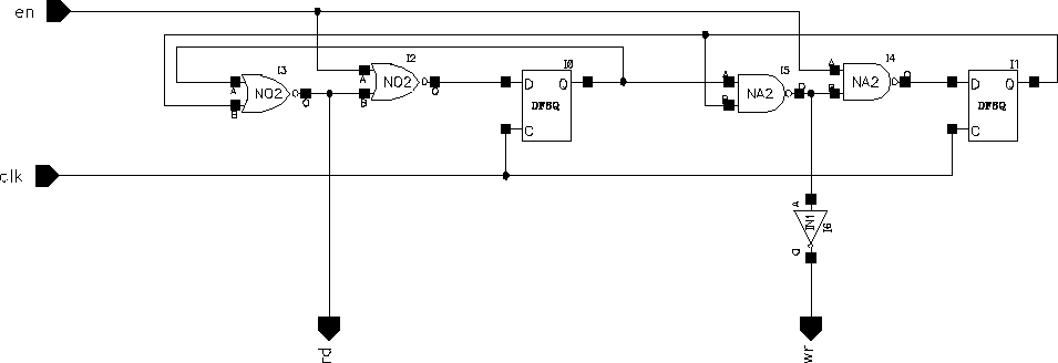 Figure 5.13: Read-Write state machine.
Aries uses a 2:1 multiplexer to achieve time domain multiplexing. A 3:1 multiplexer can be used to account for the write state where the address lines are supplied externally. As an alternative, a simple counter could be added in to the design to generate the addresses during a write cycle. These issues are discussed in Section 7.2.1
The layout of a single RAM column has evolved considerably during the design process. Figure 5.14 compares the initial floorplan to the final floorplan.
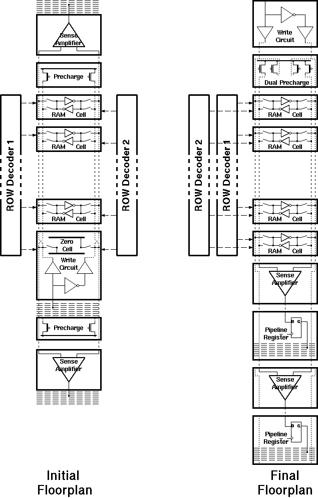 Figure 5.14: Floorplan of the RAM column.
The initial floorplan tries to take advantage of the symmetric nature of the dual port architecture in which sense amplifiers and the pre-charge circuit of the other port is placed on the ends of the blocks. The first row of the RAM will always contain the value 0. A special cell consisting of this "zero-RAM Cell" and the write circuit was designed. This cell also switched the order of the bitlines which enabled using the same pre-charge and amplifier circuits. Although the idea is appealing at first sight, it creates a few additional problems:
The final floorplan has the write circuitry on one end of the block while two read ports are on the same side. This minimizes the routing for the next adder stages. The routing of the outputs requires ten Metal-2 busses to be placed after the sense amplifier block (as there are ten outputs). It was possible to place the pipeline registers underneath these busses, which saved a significant amount of silicon area.
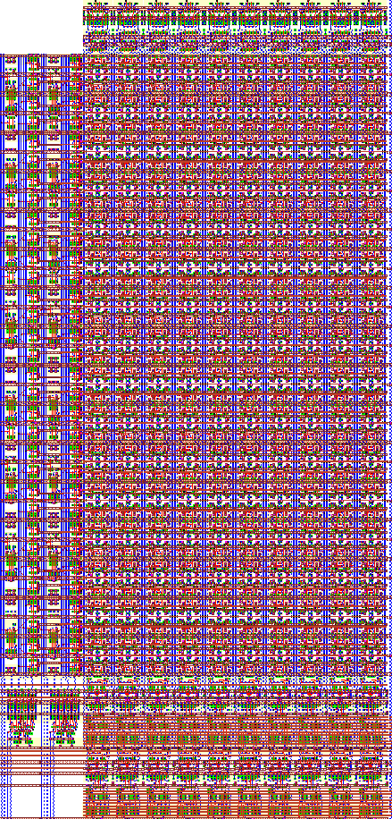 Figure 5.15: Floorplan layout of the complete Dual-Port SRAM. Detailed layout
of the circled area is shown in Figure 5.16.
Figure 5.15: Floorplan layout of the complete Dual-Port SRAM. Detailed layout
of the circled area is shown in Figure 5.16.
Figure 5.15 shows the complete layout. A close-up (marked with the circle on the complete layout) can be seen in Figure 5.16. The closeup shows parts of the first stage and second stage row decoders, the RAM cell array, the pre-charge circuit, the sense amplifier as well as the pipeline registers underneath the output bus. (the Metal-2 lines are drawn only as outlines as otherwise they would obstruct the view to the cells completely).
The layout of a single RAM block consisting of two separate address decoders, 32 rows of 10 Dual port SRAM cells, all the associated sense amplifier, write, precharge circuitry and the pipeline registers occupies an area of 390um x 815um (0.32mm^2). With these dimensions the RAM block is by far the most area consuming of all the Aries blocks. This was already predicted in the pre-design floorplan shown in Figure 4.3.
 Figure 5.16: Close-up of the Dual-Port SRAM layout (area highlighted in
Figure 5.15).
Figure 5.16: Close-up of the Dual-Port SRAM layout (area highlighted in
Figure 5.15).
 KGF
KGF