Aries: An LSI Macro-Block for DSP Applications
![[PREV]](PIC/back.gif)
![[TOC]](PIC/toc.gif)
![[NEXT]](PIC/fwd.gif)
This section presents the design methodology used for the design of various blocks within the Aries architecture, with a specific focus on full custom design of high-performance arithmetic units.
A successfull design has to satisfy a number of performance criteria as described in a so called "design specification". A design specification typically describes and sets minimum/maximum limits for the following performance criteria:
and defines a set of functions that the finished design is required to realize. As long as these requirements are met the design is said to be successful. If the design specifications are set in a conscientious manner, there should be no need to further improve any of the performance criteria beyond the limits described by the specifications, especially since this improvement will typically be at the expense of extra design time. Thus, a design that could operate at faster speeds than the given specifications is not necessarily more successful than a design that works within the limits specified.
The increasing improvements in integrated circuit manufacturing technology have resulted in smaller and faster circuits to an extent where the parasitic interconnection delays have equalled the delays of the blocks they are connected to. As a result, the dominance of aggressive speed and area requirements tends to diminish in modern designs. The high integration trend is also followed at the system level where an ever increasing market for portable devices has emerged which has increasingly contributed to the power specifications of a design.
In the 1990's the design time has established itself as one of the most dominant factors in any circuit specification. Most companies that develop integrated circuits need constant enhancements in their product line to meet the constant demand of the market. If the design is not ready on time for the market, a product from another company may address the demands and as a result the design will have missed the market.
There are various methods for designing circuits, each with its own set of advantages and disadvantages. The correct methodology for a design is based on many factors like:
![[TOP]](PIC/up.gif)
Integrated circuit design is the process of mapping a functional description of a problem on silicon so that it satisfies a set of performance criteria. The design methodology may concentrate on any level of abstraction defined within this process: From the design of actual layout masks to the high level behavioural description of the circuit. Recent literature on digital integrated circuits describe a number of distinct methodologies. All of these methodologies can be grouped into two mainstreams that differ in design philosophy:
The Top-down approach starts the design process from high-level, behavioural descriptions of blocks that will realize certain functions ,while in the Bottom-up approach the low-level elementary building blocks of the circuit are designed and combined to realize the desired function.
The logic synthesis methodology is a good example for the Top-down approach. Initially developed as a common language to describe the behaviour of digital blocks, the VHDL description of a digital circuit has soon become a widely used method for automatic synthesis of such circuits, based on a library of standart cells. This approach successfully shields the designer from the complexities of physical design and thus, speeds up the process. Yet, a number of issues such as carefull speed optimization and area minimization/management can not be addressed by a straightforward top-down design methodology.
Full-custom, mask-level design of elementary building blocks, on the other hand, is a good example of the bottom-up design strategy. This approach is also limited by the fact that the overall design complexity quickly becomes very difficult to manage in larger VLSI designs.
For most efficient results, the design of complex VLSI chips should employ a combination of bottom-up and top-down strategies which is also called the "meet-in-the-middle" approach.
Full Custom design is probably the most time consuming and detailed of all the available design methodologies. It comes at an enormously high price: costly design time. Any designer attempting to employ a Full Custom design methodology must be able to provide a satisfactory answer to the following question:
" Why do I have to design this Circuit (or block) in Full Custom ?"
The usage of this costly method must be fully justified. Most common reasons for employing a Full Custom design methodology include:
Full custom design gives the designer the freedom to modify every aspect of the design to increase the performance of the circuit. While more freedom in design parameters provides ground for more optimum solutions, it also complicates this optimization process considerably. A clear focus on design goals is of much more importance in Full Custom design than in any other design style.
Even for the most simple circuit (e.g. an inverter) with pre-set electrical parameters (such as the ratios of transistors), the designer will be confronted with a lot of options on:
The designer must be able to realize the significance of his/her decisions and maintain a continuous picture of the design status in his/her mind to be able to refine these decisions.
The design of a layout starts with the definition of the signal flow. The signal flow defines on which layer and in which direction all the input, output, clock and power lines will be laid out. This flow will give the basic guidelines for the actual design of the layout. A good signal flow minimizes the connections for the block and ensures an overall compact layout.
As a simple example let us consider the signal flow for a simple inverter that will be used to invert and/or buffer a 32 bit bus running vertically in Metal-1 in a double metal process. Figure 8.1 shows an example signal flow.
 Figure 8.1: Signal flow for a simple inverter.
The reasoning behind that signal flow is simple. The main aim is to buffer or invert the bus signals so the input must follow the direction of the bus and should preferably be on the same layer as the signal. Every cell will need power and ground connections, a different layer (Metal-2) is chosen to avoid intersections with the signal line. A narrow block is more desirable as this block will be repeated along the X axis. Figure 8.2 shows three different layouts for the inverter cell.
 Figure 8.2: Three different inverter layouts based on the signal flow shown in
Figure 8.1.
Figure 8.2: Three different inverter layouts based on the signal flow shown in
Figure 8.1.
Notice how many different solutions we can come up with for a design with fixed electrical characteristics and signal flow. The first layout in Figure 8.2 is what we can call a traditional design. The second layout has the same structure and still is in accordance with the signal flow (only the input is still in Poly not in Metal-1) the only difference is that the power connections have moved toward the center of the cell. The third layout is a radical approach, in an attempt to make a narrower cell. The third cell does not follow the signal flow exactly, as the power connections are in Metal-1 instead of Metal-2. Although at first sight this seems to be against the aforementioned signal flow rules, it is not a crucial infringement. In fact, the signal flow picture can be refined, noting that: ("It is also possible to use Metal-1 for the supply connections if layout three is used"). Notice that the wider pMOS transistor of the inverter in the third layout has been realized by a parallel connection of two small pMOS transistors.
At this stage, the third layout seems to be a better candidate, as the width of the layout is clearly less than the other two. Let us continue and try to build the inverter block.
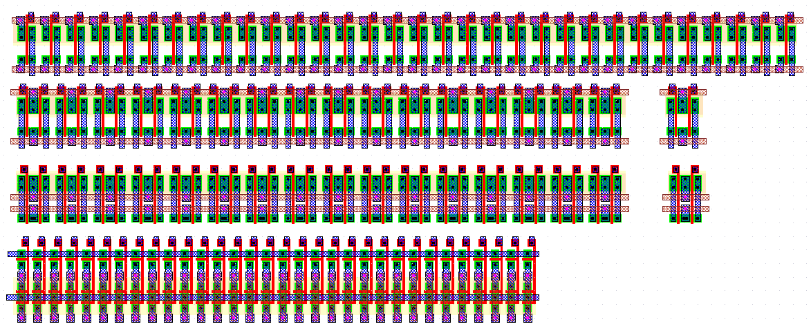 Figure 8.3: 32 inverters placed side by side.
Figure 8.3 shows four different arrangements of the inverters. The first row is a simple repetition of the first layout. It is the largest of all solutions with dimensions of 285um x 23.5um (6697.5um^2). This area can be reduced using the following trick: A close inspection of layout 1 (and layout 2) reveals that the VDD and GND connections of the layout is on the left. These connections can be shared between two adjacent cells by simply mirroring the second cell. The second row in Figure 8.3 shows the result. The combined-cell consisting of a normal and a mirrored cell is shown at the end of the row. Notice that the inputs are not evenly spaced on this row. The second occupies less than 80% of the area of the first row with dimensions: 225um x 23.5um (5287.5um^2). The third row is generated by using the second layout. This cell is very similar to the first layout and can use the same mirroring scheme. The inputs which were in Poly in the single cell however have a higher degree of freedom and are placed afterwards evenly on this row. Although the second and third rows have the same width, the base cell of the third row is slightly smaller and as a result the third row occupies less area than all the others 225um x 21.5um (4837.5um^2). The last row shows the placement of inverters from the third "narrow" layout. This row of inverters is by far the most narrow of all, but with the dimension of 190um x 30.5um (5795um^2) occupies more area than all but the first row.
Let us continue our example in which we develop a 32-bit parallel buffer, where each buffer element consists of two cascaded inverters. The layouts of three buffer rows based on three different inverter designs can be seen in Figure 8.4.
 Figure 8.4: Three different layouts of 32-bit buffers, based on the inverters
shown in Figure 8.2.
Figure 8.4: Three different layouts of 32-bit buffers, based on the inverters
shown in Figure 8.2.
The first row is generated with the first inverter layout and has dimensions of: 225um x 40.5um (9112.5um^2). The reason for the reduction in height is again a mirroring trick: The ground connection that was running at the bottom of the cell was shared between the first and second inverter. This required a small re-arrangement in the input and output pins. The second row uses the second layout and is slightly larger with dimensions of: 225um x 44.5um (10012.5um^2). The mirroring trick could not be employed here as the basic cell of the second row does not have common lines at the bottom or top of the cell. The third row is still the most narrow block but occupies more area than the two other rows: 190um x 61um (11590um^2). It seems that despite the overall larger area, Next we demonstrate that the area occupied by interconnection lines may also play a very important role. Figure 8.5 shows a 32-bit minimum width Metal-1 bus that is connected to a row of inverters, placed side-by-side. The area used to match the bus to the inputs of the inverters is almost twice the size of the inverter block, 55um x 190um (10450um^2) !
 Figure 8.5: 32-bit Metal-1 bus connecting to a row of inverters placed side-by-side.
Most of the time the signal connections and routing will have a high impact on the overall area. Especially for blocks that have large number of connections the area required for signal routing might be even larger than the active area itself. Following the example we can deduct some basic guidelines for the layout of basic building blocks:
A full custom designer actually designs the layout masks that will be used in the manufacturing of the chip. All layers in the process have some restrictions on their size, aspect ratio or separation, as a result of different physical, chemical, lithographic process limitations as well as electrical properties of the device. These rules are defined in design rules. Basically, the process manufacturer guarantees that the layers will be manufactured correctly only if these rules are followed.
Different processes have slightly different rules for their technology which makes it difficult to find unique guidelines for compact layouts. Depending on the technology, one or more of the following items (rules) may impose the most restrictive limits in a full-custom design.
nMOS-pMOS separation:
Two transistors of different characteristics
need to be manufactured on a common substrate in CMOS design. Depending
on the substrate type one, (or even both) of these transistors are
manufactured in a well that has the appropriate doping concentration.
As a result the pMOS and nMOS transistors usually need to be separated
by a large distance margin. Traditional cell design places all pMOS
transistors in a common well and all the nMOS transistors below an
imaginary line separating both regions. Generally speaking, all CMOS
designs have a large connectivity between nMOS and pMOS transistors.
In order to have a more compact layout, two or more of these pMOS-nMOS
rows could be stacked on top of each other. As pMOS-nMOS spacing is
more than the spacing between same-type transistors a common trick,
is to change the ordering of the rows (resulting in a nMOS-pMOS-pMOS-nMOS
configuration). Both of these alternatives can be seen in Figure
8.6.
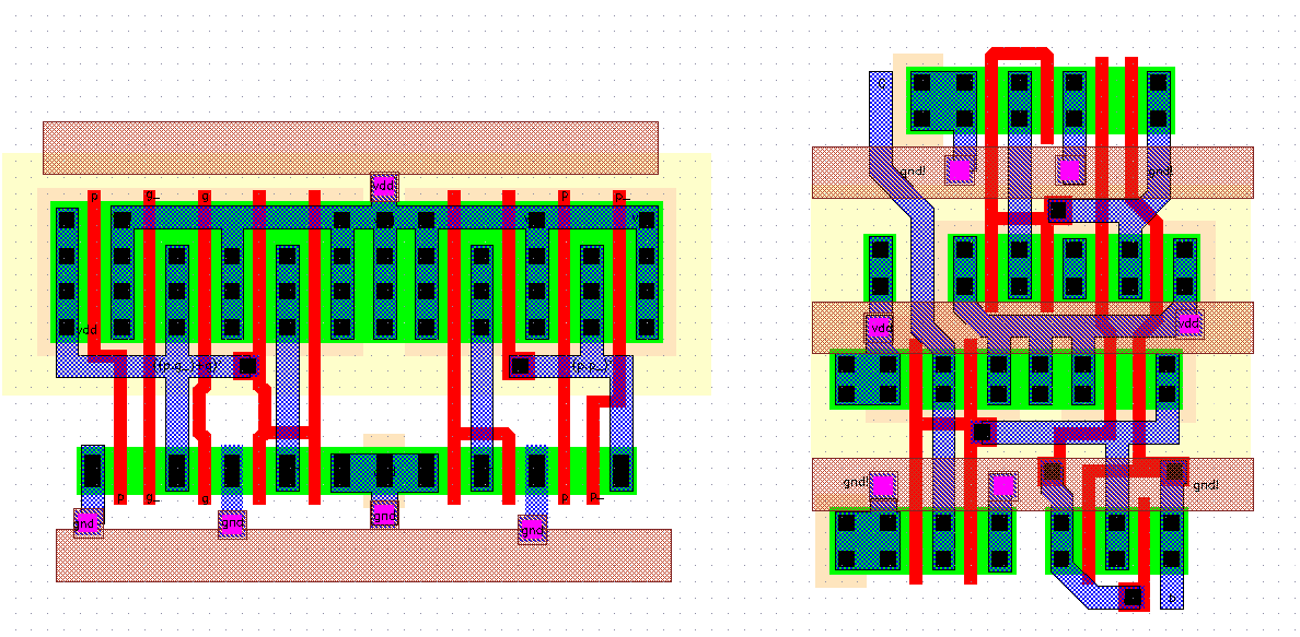 Figure 8.6: Two alternatives of nMOS-pMOS transistor placement in a cell: Traditionalplacement
where all pMOS transistors are grouped on top and all nMOS transistors
are grouped on the bottom (left), Stacked placement where alternating
rows of nMOS and pMOS transistors are placed on top of each other
(right).
Figure 8.6: Two alternatives of nMOS-pMOS transistor placement in a cell: Traditionalplacement
where all pMOS transistors are grouped on top and all nMOS transistors
are grouped on the bottom (left), Stacked placement where alternating
rows of nMOS and pMOS transistors are placed on top of each other
(right).
Substrate Contacts:
The substrate on which the transistors are manufactured
must be kept at certain voltage levels for proper operation, and in
particular, to avoid latch-up problems. An N-well (or substrate) in
which pMOS transistors are realized, needs to be biased at the most
positive voltage (VDD for example) while a P-well (or substrate) needs
to be biased at the most negative voltage (GND for example). The structures
that connect the supply lines to the substrate are called substrate
contacts. These contacts, depending on the technology, could require
a considerable area especially for small designs. A good solution
is to try to share these substrate contacts underneath the supply
connection with neighbouring cells.
Interlayer connections:
There are a number of conduction layers in
any technology (such as polysilicons, Metal-1 and Metal-2). These
layers are separated with insulating SiO2 layers. Any connection between
these layers requires a vertical link (hole) through the insulator
which are called via's (for inter-Metal connections) or contacts.
Both layers must cover this hole to a certain extent. Combined with
the width of the contact or via hole and the required extension, the
area needed to make a transition from one layer to the other can be
much larger than the minimum drawing widths of the conduction layers.
Similarly, making multiple connections between three or more layers
may result in severe area penalty, unless the technology allows stacked
via's. Additional problems arise when these contacts are required
to have a certain distance to other layers. For cell design, the basic
problem is to connect the terminals of a number of transistors. As
only Metal-1 is used for drain and source contacts, and all signals
to the gates must be connected to poly lines, almost all signals have
to be carried down to these layers. The restrictions might make using
other layers for intercell routing unfeasable.
Varying pitch of metal lines:
For a given technology, different Metal
layers may have different pitches (pitch = minimum repetition distance
of a layout pattern). Combined with the problems described for interlayer
connections, this would require that busses that are going to be routed
using these layers will have a pitch that is dictated by the pitch
of the widest layer.
45 degree routing:
The majority of automatic tools and algorithms
are based on orthogonal (i.e. x- and y-direction) connections only.
Yet, it is also evident that if signal connections could be made as
a straight line from one point to the other, the connection distance
and all associated parasitics would be minimized. Drawing structures
with free angles that conform to the design rules is an extremely
complicated task and the computational complexity for Design Rule
Check (DRC) programs increases to impractical levels. 45 degree routing
is a trade-off between these two extremes: for some connections the
connection distance could be much shorter and following rules is not
much complicated than the orthogonal rules. Most technologies allow
the designer to use 45 degree features, at least in the conduction
layers. While using 45 degree features could reduce the area of a
cell to some degree, it is not completely problem-free. Especially
for technologies where contacts and/or via's are not allowed to have
45 degree features, this technique is severely limited. Another interesting
aspect is that the area that has been saved by the 45 degree features
can (for most of the time) only be utilized by other blocks that also
have 45 degree features.
A typical Full Custom design cycle for a block starts with the circuit-level schematic of the design. Repeated transistor level simulations are used to satisfy all functional and electrical requirements for the block. The designer then draws the most efficient layout (which is expressed in terms of design time, area and speed). The electrical devices and parasitics are then extracted from this layout, which is simulated to see if the design goals were indeed met. The post-layout simulation is considered to be the most accurate verification of the design, prior to manufacturing, as it contains all the parasitic effects associated with the particular layout of the circuit. While these simulations are more detailed than the pre-layout simulations, the input data provided by the circuit extraction program which has some known limitations.
The extraction algorithms typically use very simple algorithms to measure the size of specific structures. The extraction of device parameters is no exception. Figure 8.7 shows three different transistors.
 Figure 8.7: Three different transistors with the same extracted parameters.
Even the most advanced extraction algorithms would extract these three transistors with the same parameters (W=18um, L=1um), as the algorithm simply calculates the overlap of poly line with the diffusion pattern. Yet, these transistors will have radically different behaviours in real life. The first transistor (left) is a proper 18um transistor where the channel current will flow strictly across the channel . For the second transistor (middle), the effective channel will be narrower and longer than the one that the geometry suggests Since the carriers (electrons) must travel a longer distance through the channel, following a diagonal path from source to the drain contact. The third example (right) shows another extreme condition. Here the majority of the current will flow in an effective channel that is much smaller. At any case, the actual electrical behaviour of these transistors will be quite different from each other, but the post-layout simulations will fail to reveal these differences and treat all three transistors the same.
The design of the circuit schematic is usually based on electrical requirements and is an optimization process. The most important tool during this optimization is the simulation. The result of the optimization is a schematic that has defined values for the active devices. The layout is then drawn to convert this schematic into an actual circuit.
The full custom design methodology gives the designer a great level of freedom during the design. This freedom should also be exploited during the conversion of a schematic into a layout. For example, it is not very efficient to draw many transistors of different size. This is true especially for transistors of the same type that are connected to each other. Attention must be given to reflect the dimensioning of the schematic as close as possible, but especially for digital circuits, there is no good reason for trying to stick to exact, pre-defined numbers.
The choice of the circuit schematic can be very important. For some common blocks there are many different alternatives with varying advantages and disadvantages. As an example, XOR and MUX type circuits are hard to realize in standart CMOS logic whereas in Pass transistor logic their realization is quite simple. A very interesting design style for efficient layouts is the branch based logic style [4]. The branch based logic style is a special case of the standart static CMOS designs where both the nMOS and pMOS block of the circuit are designed using parallel branches of series-connected transistors between the VDD (or GND) and the output node. An example circuit schematic comparing the Static CMOS logic to the Branch Based Logic is given in Figure 8.8
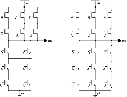 Figure 8.8: Schematic comparing the static CMOS logic to the Branch Based Logic.
Note that both circuits perform the same logic function
 (8.1)
(8.1)
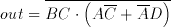
At first sight the Branch Based logic realization (right) does not look like an optimum solution as it needs more transistors than the standard static CMOS (left) version. When we compare the layouts of both blocks shown in Figure 8.9, the advantages of the Branch Based Logic can be seen more clearly.
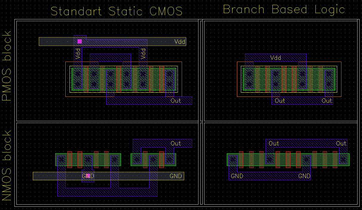 Figure 8.9: Layouts comparing static CMOS logic to the Branch Based Logic.
The structure of the Branch Based Logic is very simple and does not have any exceptions. All blocks have a single power line and a single common output line. The most important property is that the diffusion region does not have any interruptions. The pMOS network of a Branch Based Logic realization is not the topological dual of the nMOS network, but it is very easy to calculate the two networks from a simple Karnaugh map as shown in Figure 8.10. Note that both the nMOS and the pMOS block functions are minimized strictly in the sum-of-products form.
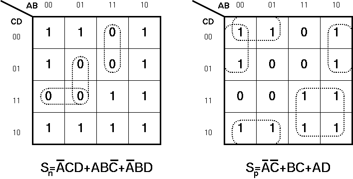 Figure 8.10: Karnaugh map for Branch Based Logic realization.
The nMOS networks is generated by using the sum of products representation from the Karnaugh map by selecting the "0" cubes. The pMOS network is selected by a similar way but the "1" cubes are selected, but as a pMOS transistor is turned on by a logic "0" on its gate, all the variables are inverted.
This section will discuss some aspects of the design of the Systolic Adder in detail to illustrate the design methodology employed throughout the design of the Aries architecture.
The first step after having a complete functional description is to come up with a functional schematic. The schematic given in Figure 6.12 was the first schematic designed to test different components, especially the final carry propagate adder. This gate level schematic is repeated in Figure 8.11 for reference. The whole schematic consists of standart cells and gives a good overview of the connections and complexity. The concept and some difficult test cases can be simulated to verify the functionality. The final carry propagate adder is designed as a separate subblock which can be replaced on the top-level schematic easily. The same schematic is also usefull while evaluating the post-simulation results and generating test cases.
 Figure 8.11: Schematic of the Systolic Adder.
The basic building block of the systolic adder block is the one-bit FA, therefore an area efficient and high-speed FA cell is the key to the fast systolic adder. As the whole block is expected to perform an operation within 10 ns, initial studies showed that a delay of little over 1ns. per FA was needed. In order to avoid potential difficulties of syncronization and timing a dynamic CMOS alternative was ruled out at the outset.
There are many different realizations of the static CMOS one-bit FA. The alternatives can be classified into two main groups, i.e., adders based on Pass Transistor Logic and adders based on conventional (standart CMOS) logic.. As the FA structure uses XOR based functions, it is well suited to Pass Transistor logic. The pass transistor logic alternatives indeed produce some compact solutions [22] but the outputs may produce more glitches than standart CMOS alternatives. Additionally, as all the remaining parts were to be designed using the conventional static CMOS logic, it was decided not to use pass transistor logic based adders.
There are two basic standart CMOS realizations of the FA. The one shown in Figure 8.12 has some logic optimization to use a Carry' in the calculation of Sum and is faster than the standart alternative which consists of two separate sub-circuits for the realization of Carry and Sum.
 Figure 8.12: Circuit schematic of the CMOS FA.
The first step in creating an optimized schematic is to draw a circuit that only uses minimum-width transistors and investigate the response. It is not always very easy to calculate a worst case for a given circuit. A well designed FA has a worst case delay when both of its outputs change. This happens when the number of logic "1" inputs change from 2 to 1 or from 1 to 2. The optimization problem is not only the problem of minimizing this delay, but also making sure that the conditions for the worst-case remain the same in the optimized circuit. Figure 8.13 shows simulation results of a FA circuit consisting of minimum-size transistors.
 Figure 8.13: Transient operation of a CMOS FA consisting of minimum-size transistors.
It can be seen that the worst case delay is almost 2 ns (please note that the delay of Carry-out is much shorter). This delay can now be optimized (reduced) iteratively, by running a number of simulations and adjusting the transistor sizes according to the simulation results. We know that in all static CMOS circuits, a rising output transition is caused by one of the pMOS branches, where a falling output transition is always caused by one of the nMOS branches. The delay associated with a certain transition is dictated by the strength (or weakness) of the corresponding branch. Thus, with the help of some simulations, the designer can identify which branches are responsible for particular outputs. This will enable the designer to modify the dimensions of only the relevant transistors. There some simple rules of thumb that should be followed:
The dimensions listed in Table 8.1 were used for the optimized FA circuit.
Table 8.1:Transistor sizing for the FA.
              nMOS    pMOS

Carry Block   5.3um   10.8um
Sum Block     4.2um    6.4um
Inverters     4.0um    8.4um
The Carry block has larger transistors since the output of this block also drives the Sum block. The simulation result shown in Figure 8.14 shows that the design goals are indeed met by these dimensions.
 Figure 8.14: Transient operation of the optimal FA circuit.
The worst case delay is close to 1 ns, almost 50% less than that of FA circuit with minimum-size transistors.
The first step of the layout is to create a signal flow graph that shows the connection directions and the general layout of the cell. A number of factors need to be taken into account:
After creating the signal graph, the transistors have to be placed. The emphasis is to have a block that is as narrow as possible. It usually does not pay off to break up transistor blocks that form a branch. In the FA layout, the branch for the sum calculation produces the widest diffusion block. This gives a limit for the minimum width of the block, as it is not possible to make a narrower block without breaking up that branch. Next, the other branch blocks are placed. Since the FA uses mostly the three input signals for all of its blocks it is possible to put two nMOS and two pMOS blocks one after another (generally a mirroring approach illustrated in Figure 8.6 is used). The output inverters which are totally separated from the remaining blocks are placed at the very bottom of the block in a mirrored scheme. Another alternative is to place them to one side of the Adder, which would increase the width of the block.
The third step is to make the connections and finalize the layout. All three steps of the adder layout are shown in Figure 8.15 The complete layout of the FA cell has dimensions of 60.2um x 24.4\um and occupies an area of 1468um^2.
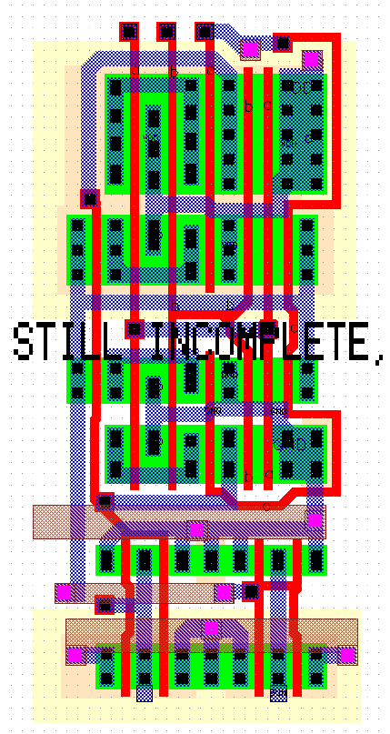 Figure 8.15: The signal flow graph(left), rough placement(middle) and final layout(right)
of the FA ( not complete ).
Figure 8.15: The signal flow graph(left), rough placement(middle) and final layout(right)
of the FA ( not complete ).
The circles on the final layout show the connection points for a ripple carry configuration. During the design of the final layout, a few additional enhancements were made:
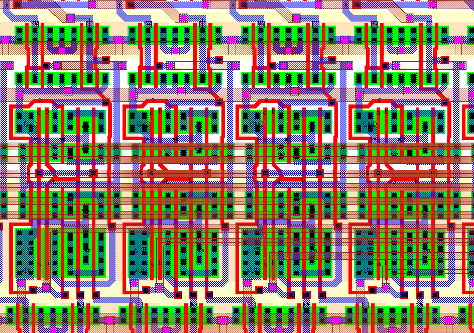 Figure 8.16: Placement of the designed FA cells within the second row of the systolic
adder array.
Figure 8.16: Placement of the designed FA cells within the second row of the systolic
adder array.
Figure 8.16 shows a close-up view several FA's as they are placed in the systolic adder array. The figure shows four FA's and neighbouring structures on the second row of the systolic adder array. The carry-save connections from the bottom of the row, the connection and sharing of the VDD lines between two cells (the cells are placed upside down) and the bus running over the cell are clearly visible.
A post layout simulation result of the FA is shown in Figure 8.17. The results differ only slightly from the simulation results obtained by using the schematic representation. The worst case delay is still around 1 ns.
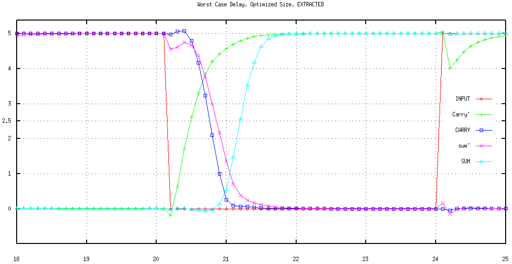 Figure 8.17: Transient operation of the optimized FA circuit, post-layout simulation.
The first two FA rows of the systolic adder produce two 10 bit numbers that need to be added for the final result. After it was decided that a Ripple Carry Adder was not suitable for this task, a number of alternatives were evaluated. The Brent-Kung Parallel Prefix Adder structure was found to be the most suitable adder structure for this application.
Although the Adder operates on 10-bits, due to the negative number processing enhancements, the final Carry-out signal is not required, thus the adder effectively uses the carry propagation scheme of a 9-bit Parallel Prefix Adder. Figure 8.18 shows the graph representation of the (semi) 10-bit Brent-Kung Parallel Prefix Adder.
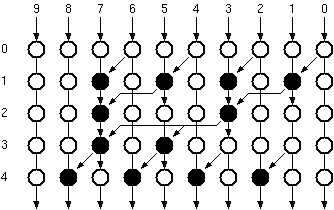 Figure 8.18: Graph representation of the (modified) 10 -bit Brent-Kung Parallel
Prefix Adder.
Figure 8.18: Graph representation of the (modified) 10 -bit Brent-Kung Parallel
Prefix Adder.
The schematic for this arrangement was drawn first. An alternative schematic that used alternating And-Or-Invert (AOI) and Or-And-Invert (OAI) gates for Delta cells was also evaluated. These gates are simpler to build with static CMOS, but they were not very suitable for this particular application. Each AOI based Delta cell had to be followed by a OAI based Delta cell, if the outputs of two different Delta cells (one AOI and one OAI) drive another Delta cell (which is the case for some of the Delta cells) two inverters are necessary to correct the p and g signals. On a second note, for the majority of the cases a static CMOS gate with a built-in inverter performs better than a static CMOS gate without an output inverter.
As discussed earlier, a parallel prefix adder consists of three main parts: The preprocessing stage which is essentially a NAND gate and a XOR gate, the post Processing stage which is a simple XOR gate (the pipeline DFF was also added to this stage), and the carry propagate stage which consists of a network of Delta cells. These three blocks need to be designed separately.
This stage consists of two simple gates. The AND stage is quite straightforward, but the XOR function is more complicated. The basic CMOS realization of the XOR gate requires 10 transistors, and both the input signals and their complements. A novel XOR gate with only 6 transistors (including the output inverter) was used instead of the static CMOS alternative [26]. Figure 8.19 shows the circuit schematic of this XOR gate.
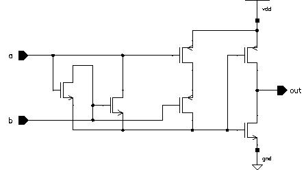 Figure 8.19: Circuit schematic of the Wang XOR gate.
Since the preprocessing stage drives more stages, all transistors in this stage are designed to allow faster operation. These cells are placed on top of a row of FA cells. It is very important that the pitch of these cells matches the pitch of FA cells. Otherwise, each block would need to be connected separately and the resulting routing would have significant area overhead.
The basic graph of the 10-bit parallel prefix adder in Figure 8.18 shows that four rows of delta functions would be necessary to realize the carry propagate function. It was also considered to use only three rows (as two rows only needed 2 Delta cells while the remaining two rows used 4 cells). The problem lies in that the output of these cells have to be fed into the next stage. When the Delta cells are not placed in their rows this would mean re routing the signal backwards. It was found that this solution would work for certain cases (it was used in the accumulator which uses four rows instead of the required five ) but would complicate the routing and generality of the circuit too much. As at most 4 blocks per row are used, these blocks are designed to be two times as wide as the preprocessing blocks and their height was minimized.
This cell again must match the width of the FA cells. It consists of the same XOR that is used for the preprocessing stage (with smaller transistor dimensions) and a pipeline register which is the same DFF that is used throughout the design with slight modifications to have the required width.
Figure 8.20 shows the layouts of the three basic cells that are used in the Parallel Prefix Adder.
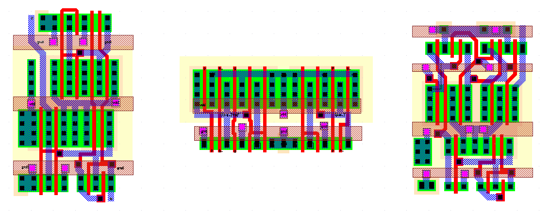 Figure 8.20: Layouts of preprocessing cell(left), Delta cell(middle), postprocessing
cell (right) of the Parallel Prefix Adder.
Figure 8.20: Layouts of preprocessing cell(left), Delta cell(middle), postprocessing
cell (right) of the Parallel Prefix Adder.
The problem with the negative numbers and the solution was discussed in Section 6.1.4. The necessary logic cells (AND gates) can easily be added to the circuit and do not require any special design effort. Figure 8.21 shows the 3 AND gates that have been placed in front of the first row of FA's.
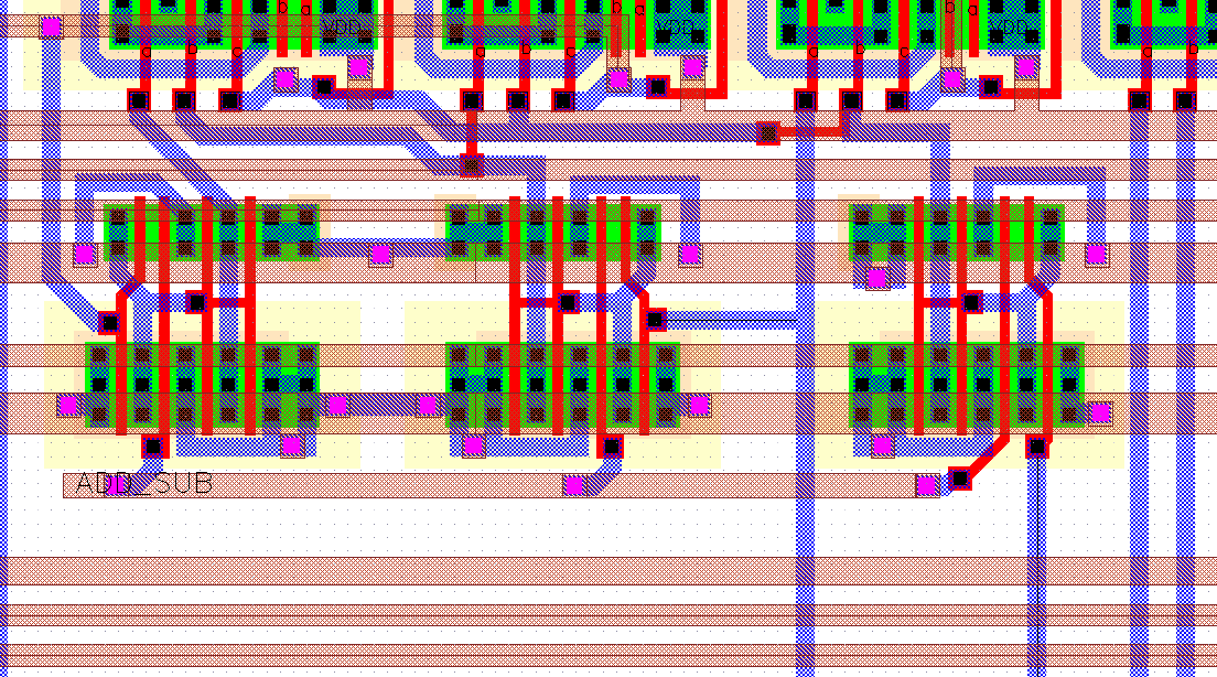 Figure 8.21: Blocks inserted for negative numbers.
The Metal-2 lines to the bottom of the picture are the data inputs while the Metal-2 lines covering the AND gates are used to connect the Clk, Read and Read' signals of the Sense amplifiers between the two RAM blocks cells as well as the VDD and GND connections.
The systolic adder has also been described simulated and synthesized by a top down approach using VHDL (VHSIC Hardware Description Language) . The code given below was written for this purpose:
There are different methods for describing a behavioural model. The most simple one would involve the shifting and addition of four 10-bit numbers. The resulting code includes registers for individual operations so this description is not very useful. A more hardware level approach would be to describe the connections of various components which would correspond to literally describing the schematic. The method chosen here uses variables to force the synthesiser to generate a layout that performs these operations one after another without using registers to store intermediate results.
The circuit was simulated, verified and synthesized. The basic core area occupied by the synthesized standart cells is 500um x 420um (210.000um^2) \)which is more than double the size of the full custom solution. This comparison may still not be very fair for a few reasons:
There are important advantages of the synthesis approach. Designing the adder using the synthesis approach takes about one tenth of the time used to design a Full Custom Block. Furthermore, process migration is much simpler in the synthesis approach, changing a simple option within the synthesis environment is enough to map the design to a new technology (provided that standart cells exist for that technology). These two arguments are commonly used to describe the superiority of the synthesis approach.
For random logic structures, the synthesis- approach is simply unbeatable. For regular structures such as datapaths, systolic arrays and storage elements the verdict is not so clear. While the algorithm is mapped much faster into a gate level netlist, the actual placement and routing of these standart cells is much more complicated in a synthesized design. A full custom block is always designed with the signal flow and overall floorplan in mind, and the cells are designed to fit into the floorplan. The syntesized gate netlist on the other hand, contains no information and optimization about the signal flow and shape of the block. A second EDA tool has to be used to make the placement and routing of the actual design. The designer does not have direct access to the design (as the gate level netlist would not mean very much to the designer) and has to rely on this high level tool to make the routing. For a high performance design, the placement and routing step can take much longer design effort than writing the hardware description. New design tools try to address this problem in which sophisticated expert systems try to determine a-near optimal floorplan, automatically breaking the design into sub-blocks and setting optimization parameters for the synthesis of these blocks.
Full Custom design (for the design of regular structures) is not as difficult as some sources suggest it to be. As an example, the whole Aries block consists of the following design elements (only cells that are introduced in the stage are listed) :
This makes a total of 13 different blocks. The most complicated block that is listed here is the FA which has 28 transistors, all of the remaining blocks are much smallerwith respect to transistor count (at least five of the blocks described above can be called elementary blocks). Furthermore, any designer that employs a full custom design technique has most likely designed a number of different variations for most of the basic cells, thus only a few blocks have to designed from scratch. Even the cells that need to be re-adjusted to fit a certain area or meet a speed constraint, benefit from the design experience from earlier (similar) designs.
Speed optimization is another issue. First of all, the full custom designer has complete control over the design, and can make any adjustment that he/she feels necessary and can therefore determine all the critical factors that affect the operation speed such as block placement, interconnection and device sizing, precisely. As for the majority of the circuits, only a few cells (the ones that are on the critical path) need to be optimized for speed, this is also not a very difficult task.
Overall, for the design of regular structures the full custom layout design technique is not as obsolete as many sources would suggest. It offers the highest performance both in terms of area and speed, and the design time for high performance designs is comparable to that of synthesized designs, which have typically much lower performance.
 KGF
KGF