GALS System Design:
Side Channel Attack Secure Cryptographic Accelerators

Frank Kagan Gürkaynak
 
<kgf@ieee.org>

 
Disclaimer:
This is the www enabled version of my thesis. This has been converted from the sources of the original file by using TTH, some perl and some hand editing. There is also a PDF. This is essentially as it is, but includes formatting for A4, and some of the color pictures from the presentation.

Contents

1  Introduction
2  GALS System Design
    2.1  Design Styles
        2.1.1  Synchronous Design
        2.1.2  Asynchronous (Self-timed) Design
        2.1.3  GALS
    2.2  The GALS Methodology
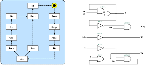
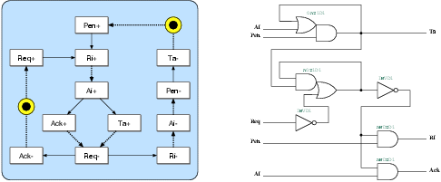
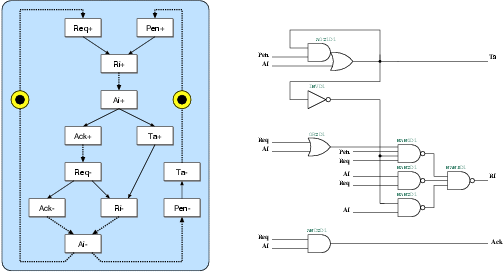
        2.2.1  Port Controller Types
        2.2.2  Local Clock Generator
        2.2.3  Timing Constraints
    2.3  GALS-Based Solutions
        2.3.1  Low Power
        2.3.2  High Performance
        2.3.3  Ease of Integration
        2.3.4  Secure Applications
3  Cryptographic Accelerators
    3.1  A Cryptology Primer
    3.2  Advanced Encryption Standard (AES)
    3.3  AES operations
        3.3.1  AddRoundKey
        3.3.2  SubBytes and InvSubBytes
        3.3.3  ShiftRows and InvShiftRows
        3.3.4  MixColumns and InvMixColumns
        3.3.5  Key Expansion
    3.4  AES Hardware Implementations
        3.4.1  Datapath Width
        3.4.2  Encryption/Decryption
        3.4.3  The AES Round Organization
        3.4.4  Roundkey Generation
        3.4.5  Comparison of AES chips
    3.5  Cryptographic Security
        3.5.1  Side Channel Attacks
        3.5.2  Differential Power Analysis
        3.5.3  Countermeasures Against Side Channel Attacks
        3.5.4  Implementation Issues
4  Secure AES Implementation Using GALS
    4.1  Partitioning
    4.2  DPA Countermeasures
        4.2.1  Noise Generation
        4.2.2  Operation Re-Ordering
        4.2.3  GALS Modules
        4.2.4  Variable Clock Periods
        4.2.5  Security Effort
    4.3  Realization and Results
        4.3.1  David
        4.3.2  Goliath
        4.3.3  Interface
        4.3.4  Random Number Generation
        4.3.5  Reference Design
        4.3.6  Physical Implementation
        4.3.7  Simulation Results
        4.3.8  Measurement Results
5  Designing GALS Systems
    5.1  Design Automation Issues
    5.2  Designing Asynchronous Finite State
Machines

        5.2.1  Port Controllers in Acacia
        5.2.2  Data Exchange between David and Goliath
        5.2.3  Data Exchange between Goliath and Synchronous Interface
    5.3  Testing Acacia
    5.4  Adapting Modules for GALS
    5.5  Related Research Directions
        5.5.1  Network-on-Chip Systems
        5.5.2  Dynamic Voltage and Frequency Scaling
        5.5.3  Latency-Insensitive Design
6  Conclusion
    6.1  Cryptographic Hardware Design
    6.2  GALS Design Methodology
    6.3  Final Words
A  'Guessing' Effort for Keys
B  List of Abbreviations

Abstract

The integrated circuit manufacturing technology improves almost daily, and enables designers to construct circuits that are both smaller and are able to work faster. While this increases the performance and allows more functions to be integrated on to micro-chips, it also poses significant challenges to designers.
Conventional digital circuits rely on a global clock signal to function. These circuits are called synchronous, as the timing of all operations of the circuit are derived from the global clock signal. As a result of the technological improvements with each new generation of integrated circuits, both the clock rate, and the number of clock connections within the micro-chip continue to increase. Reliably distributing the clock signal over the micro-chip has become one of the leading challenges of modern digital system design.
The Globally-Asynchronous Locally-Synchronous (GALS) system design has been developed to address this problem. A GALS system consists of several sub-designs, called GALS modules, that have their own local clock generators. Each module by itself is synchronous and can be designed using a conventional design methodology. What is required is a reliable method to exchange data between these independent GALS modules. Instead of a global clock signal, GALS systems use an asynchronous handshaking protocol between GALS modules. Each GALS module contains additional control circuitry that briefly pauses the local clock to ensure data integrity during these transfers.
The feasibility of the GALS design methodology, and an extension of the methodology to support multi-point connections between GALS modules has been investigated in two previous Ph. D. theses by J. Muttersbach and T. Villiger. In this thesis, the GALS methodology has been applied to improve the security of cryptographic systems.
Cryptographic systems are an integral part of modern digital society providing solutions to secure information from unauthorized access. In its most basic form, a cryptographic algorithm uses a secret key (a series of 0's and 1's) to transform information so that it can only be deciphered by others who have the same secret key.
There are several well established algorithms, like the Advanced Encryption Standard (AES), that provide a very high level of security. However, once this algorithm is implemented, in either hardware or software, it acquires several physical properties (heat, power consumption etc) that can be monitored during operation. Starting in 1999, it was shown that it is possible to extract the secret key of a cryptographic system by only monitoring the power consumption. This is a very serious problem, and immediately a number of countermeasures were developed against these so-called side channel attacks.
In this thesis, the design of a GALS-based AES implementation is presented. The design consists of three independent GALS modules which have a local clock generator that is able to change its period randomly. By combining this architecture with several well-known countermeasures against side channel attacks, the security of the AES implementation has been improved considerably.
This work represents the first application of GALS to improve the side-channel security of a cryptographic system. A mature GALS design flow, which is mainly based on industry standard electronic design automation tools, has been used to fabricate the circuit. Measurement results showed that the performance metrics (throughput, area, power consumption) of the GALS integration are comparable to circuits that were designed using conventional synchronous methods.

Chapter 1
Introduction

This thesis combines two relatively different areas of research. On one hand, the Globally-Asynchronous Locally Synchronous (GALS) design methodology and on the other hand the design of secure cryptographic systems are covered in this thesis. In the end, the GALS design methodology is applied to a cryptographic system to increase its security against certain attacks.
GALS has been introduced as a design methodology that will facilitate the design of multi-million transistor integrated circuits in the future. Instead of designing a completely synchronous system where a global clock signal has to be distributed over the entire circuit with considerable effort, GALS allows individual modules to be clocked independently. This has two important consequences. The most visible result is that all problems related to global clock distribution and meeting timing constraints at the final stage of design are virtually eliminated. Secondly, the GALS methodology dictates a clear separation between functionality that is provided by the locally synchronous part, and the communication that is asynchronous. Modules designed in this way can be re-used much more easier.
The Integrated Systems Laboratory (IIS) of the Swiss Federal Institute of Zurich has been one of the leading research institutes in GALS research, especially in practical realizations of GALS systems. The Marilyn design developed as part of Jens Muttersbach's Ph.D. research is the first successfully integrated GALS system, and the Shir-Khan design developed as part of Thomas Villiger's Ph.D. research is the largest implemented GALS system to date.
Despite all these advantages GALS has so far not seen universal acceptance and has remained a niche technology at best. Among the most frequently cited reasons is the lack of design tool support and a test methodology. The GALS design flow demonstrated in this thesis uses conventional design tools for most of the design stages. Furthermore, a test methodology that combines standard stuck-at fault testing for the locally synchronous parts with a functional test for the asynchronous communication is presented. While the GALS design flow presented here may not be of industrial quality, it is not far from it.
GALS design is typically seen as a replacement for conventional design methods. It was presented as a 'fix' for clock distribution and top-level timing problems of standard synchronous design. However, GALS also offers several new and interesting opportunities to designers. In this thesis, the ability of using independent clock domains of GALS is exploited to increase the security of cryptographic accelerator circuits.
Unlike previous GALS research that was mainly project based, the experience on cryptographic hardware design started off as student semester thesis projects. Cryptographic algorithms are well suited as examples for students learning how to design digital micro-chips. The first Advanced Encryption Standard (AES) implementation at the IIS was realized during the winter semester 2001/2002. Unfortunately a post-processing error resulted in several shorts on the circuits. While the basic functionality of the chip could be verified on one sample after extensive micro-surgery, the AES algorithm was implemented a second time the following year. This implementation, called Fastcore, also included many features that were missing in the first one.
Cryptographic algorithms like AES are basically secure against algorithmic attacks. But once such algorithms are implemented, be it on dedicated hardware or as software on a micro-controller, different physical properties of the algorithm can be observed. Over the years, sophisticated attacks were developed that enabled attackers to break cryptographic devices by such observations. A very popular and extremely efficient method is the so-called Differential Power Analysis (DPA) attack that is based on observing the power consumption of a system implementing the cryptographic algorithm.
For the most part, cryptographers are not good hardware designers, and hardware designers are equally bad cryptographers. It is therefore not very surprising that chip designers, upon reading mostly theoretical papers on DPA attacks, regard them as interesting, but not really practically applicable for dedicated chips. Following such a dispute, the aforementioned Fastcore design was successfully attacked using the DPA method. This was the first successful practical DPA attack on a micro-chip implementing the AES algorithm.
In the following semesters, several other AES chips were developed as part of semester and diploma theses, each using a set of different ideas for countermeasures against similar DPA attacks. The GALS-based AES implementation presented in this thesis is a result of this continued involvement in the field of cryptographic security. Cryptographic security is a difficult problem, and it would be foolish to imagine that the approach presented here will solve the problem completely. However, it presents a fresh and different solution that could prove to be a step in the right direction.
This thesis gives a comprehensive overview of the GALS design methodology and it presents a unique implementation of the AES algorithm using GALS. The final design called Acacia is as fast as its synchronous counterpart while allowing efficient countermeasures against DPA attacks to be implemented. The GALS methodology used for the design has been refined, new port controllers have been designed, and for the first time a viable test methodology for a GALS system has been presented.
A brief overview of the GALS design methodology is given in Chapter 2. The GALS subject is then rested until the example design is presented later in Chapter 4. Before that, Chapter 3 includes a short introduction to cryptography, and it describes the Advanced Encryption Standard (AES) in detail. The AES algorithm is examined from a hardware designers view, and solutions that result in different area and throughput configurations are compared. The chapter concludes with a discussion on cryptographic security. The secure AES implementation using GALS is introduced in Chapter 4. The following Chapter 5 is dedicated to a series of topics related to GALS design. These include the design flow and test methodology as well as a discussion on how a standard synchronous design can be converted to GALS. Finally Chapter 6 presents a summary and draws conclusions.

Chapter 2
GALS System Design

The design of multi-million transistor integrated circuits is a very challenging task. And yet, the continuous improvement in the integrated circuit manufacturing technology enables even more complex systems to be designed almost every day. Just to illustrate how far current manufacturing methods have come, consider the following:
At the time of writing, commercially available micro-processors containing tens of millions of transistors were running at a clock rate of 4 GHz. During one clock period (250 ps) of such a micro-processor, light would merely be able to travel 7.5 cm in vacuum.
For several years, scientists have claimed that the present way of designing chips has reached the limit of its capabilities. At least until now, this limit has been avoided mainly by endlessly refining all aspects of the design methodology. Nevertheless, developing alternative design methodologies has remained an attractive field of study.
The Globally-Asynchronous Locally-Synchronous (GALS) design methodology has been developed to address several key problems of the widely used synchronous design methodology. GALS basically combines the well-known synchronous design methodology with the asynchronous design style. The goal is to combine the advantages of the respective design styles while avoiding their short-comings. The following is a brief description of three design styles, synchronous, asynchronous and GALS.

2.1  Design Styles

2.1.1  Synchronous Design

Today the synchronous design style is by far the most established way of designing digital circuits. The defining characteristic of a synchronous circuit is the omni-present clock signal throughout the circuit. All events in the circuit are ordered by this clock signal.
In a synchronous circuit, the clock qualifies all data signals of the circuit. The circuit operates correctly as long as all signals within the circuit have their intended values at the time of a clock event. The entire timing of a synchronous circuit is therefore defined relative to the global clock signal. Since all parts of the circuit are controlled by the same pacemaker, it is possible to have a deterministic schedule for all events in the circuit.
This design approach has been used with great success since the beginning of the digital design. As with all engineering solutions, there are several problems with the synchronous design approach. Unfortunately, recent developments in Integrated Circuit (IC) manufacturing technologies, besides increasing the performance of ICs in several orders of magnitude, has also aggravated several problems of the synchronous design style. In particular, the distribution of a global clock signal over the entire circuit has become a formidable challenge.
Since the timing of a synchronous circuit depends on the global clock signal, it is imperative to distribute the clock signal to all clocked elements in the circuit at the same time. Modern IC technologies allow circuits to be designed much smaller and to be clocked at a much faster rate. Consequently, the clock has to be distributed to more elements in the circuit with an ever increasing precision. In a modern design, a significant portion of time is spent in distributing the clock and achieving timing closure, a term used to describe that all timing conditions of the circuit have been met.
Most modern designs are designed with more than one clock signal, which complicates design to no end. The reasons for introducing additional clock signals are varied. The part of the system that communicates with the environment may be forced to use a clock rate compatible to the specific communication protocol used. Systems that have many such interfaces end up using different clocks. Modern ICs are often too complex to be designed from scratch. In the so-called System-on-Chip (SoC) methodology, pre-designed modules are combined to create highly complex systems on a single chip. The module of a SoC system may be designed under different timing constraints and may require different clocks to fulfill operational requirements.
Strictly speaking, if more than one clock is used, the system is not always synchronous. Systems can be classified depending on the frequency-phase relationship of their clocks. For an example with two clock signals, the following classifications can be made:
synchronous
Both clocks share the exact same frequency, and there is no phase difference between two clocks.
mesochronous
Both clocks share the same clock frequency, but there is a constant phase difference between two clocks.
plesiochronous
Both clocks have nearly the same frequency, but there is a small difference. As a result, the phase difference between two clocks can accumulate to an unbounded value.
periodic
There is a fixed ratio between the clock frequency of two clocks.
asynchronous
There is no frequency (or phase) relationship between two clocks.
Complex SoCs can easily have up to thirty or more separate clock signals. Not all of these clocks may share the same relationship with each other. But in most cases, portions of the design that share a single clock are designed using standard synchronous design approach. The challenge at the top level of the design is to resolve all timing conflicts between sub-designs that use different clocks. Solving the clock distribution problem for a single clock is already difficult enough, reliably solving the problems of multi-clock-domain systems is bordering on the realms of impossibility [Gin03].

2.1.2  Asynchronous (Self-timed) Design

Asynchronous circuits can be defined as sequential circuits that do not rely on a global clock signal for operation. An asynchronous circuit consists of many sub-blocks that use handshake signals to request data from connected sub-blocks, and to respond to such requests. These handshake signals are generated locally in each sub-block. Since asynchronous circuits do not rely on a global signal, they are sometimes also referred to as self-timed circuits1. To improve readability, in parts of this thesis, the term self-timed will be used instead of asynchronous.
Using a self-timed design style has several advantages:
An extensive evaluation of asynchronous design is beyond the scope of this thesis. More detailed information on asynchronous circuits topic can be found in [SF01].
Today, although it is at least as old as synchronous design, self-timed design remains to be a niche technology. Steve Furber2 has identified three important reasons why, despite all of its perceived advantages, self design methodology has not seen widespread acceptance:

2.1.3  GALS

By itself, GALS is a very general description. It merely suggests that the system consists of multiple functional blocks that communicate asynchronously. Neither the specific asynchronous communication between the blocks, nor the synchronization method used at block boundaries is determined. Therefore many different flavors of GALS have been presented in the literature:
In the remainder of this thesis, the term GALS will be used to describe the specific GALS methodology developed by J. Muttersbach [Mut01] at the Integrated Systems Laboratory.

2.2   The GALS Methodology

Figure simple_gals
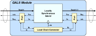
Figure 2.1: An overview of a single GALS module with a input and an output port.
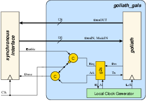
The GALS module shown in Figure 2.1 is the basic building block of a GALS system. At the heart of each GALS module is a locally synchronous (LS) island. This block contains the functionality of the module and is developed using conventional synchronous design techniques. The clock signal for the LS island is generated by a local clock generator. The data communication between GALS modules is governed by specialized port controllers. These are asynchronous finite state machines (AFSM) that can pause the local clock generator during data transfers in order to ensure data integrity.
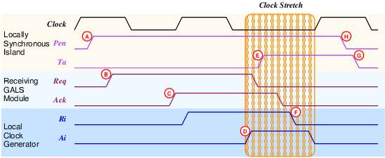
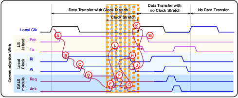
The GALS module uses a four-phase bundled data protocol to exchange data with similarly designed GALS modules. Figure 2.2 shows a timing diagram with three consecutive clock cycles of a D-type output port controller (which is later described in section 2.2.1). The LS island uses the Port Enable (Pen) signal to activate the port controller (A). The port controller immediately sends a request signal (Ri) to pause the local clock generator (B). The local clock generator issues the acknowledge signal (Ai) only after it has stopped the propagation of a new active clock edge (C). No new clock pulses will be generated after this point, which effectively freezes the LS island. The port controller then activates the Req signal (D), which in turn tells the receiving GALS module that new data is available for transfer. The port controller at the receiving GALS module goes through similar stages and as soon as it is ready to accept new data, it will acknowledge the request by activating the Ack signal (E). At this moment, the local clocks of both GALS modules are halted and the receiving GALS module can safely sample the data . Afterwards, the handshake signals are returned to their initial states and the local clocks are released. On the transmitting side Req is deactivated first (F). Once the communication partner deactivates Ack (G), the local clock generator is released by deactivating Ri (H). The local clock generator lowers Ai (J) and continues to generate clock pulses (K). The port controller also sets the transfer acknowledge (Ta) signal to notify the LS island of a successful data transfer (L).
Figure timing3
Figure 2.2: Timing for a D-type output controller for three consecutive clock cycles. In the first cycle shown, the environment is slow to react to the Req signal. As a result the clock is stretched until the data transfer has been processed. The second cycle shows another transfer where the handshake finishes within the clock cycle. Finally in the third cycle, the Pen signal is not enabled, and no data transfer is initiated.
In the communication scheme presented above, the LS island starts the data transfer by activating the Pen signal. To enable data transfers in consecutive clock cycles, Muttersbach used a two phase protocol only for the Pen signal. A new data transfer is initiated by changing the value of Pen. This can be seen in figure 2.2, in the first cycle the data transfer is initiated by a rising transition of the Pen signal (A) and in the second cycle a new data transfer is initiated by a falling transition of Pen (M). In the third cycle, Pen stays low, and no data is transferred. When compared to a four-phase realization, this arrangement doubles the throughput of the data connection at the expense of more complex port controllers.
In the first clock cycle shown in figure 2.2, the local clock is stretched as the sending module awaits the Ack signal, effectively slowing the sending module. If both GALS modules are ready to communicate, the data transfer can be completed without stretching the local clock at all as illustrated in the second clock cycle in figure 2.2.

2.2.1   Port Controller Types

The timing diagram in figure 2.2 shows an output port controller that suspends the local clock of the LS island as soon as it is ready to transmit data. This is a desired behavior for a system that can not continue without completing the present data transfer. Muttersbach named the input and output ports that halt the clock immediately 'Demand Type' (D-type) ports.
In some cases however, a GALS module may initiate a data transfer and continue operating up to a point where a data dependency occurs. The 'Poll Type' (P-type) ports were developed to serve this purpose. In contrast to a D-type output port, a P-type output port first activates the Req signal to tell its communication partner that it is ready to send data. Until an Ack signal is received the local clock is not paused and the LS island continues to operate normally. As soon as the P-type controller receives an Ack it issues a Ri signal to pause the local clock generator momentarily. Then, after the four-phase handshake is completed and all control signals return to their initial levels. For P-type controllers the Ta signal is very important as the LS island needs to constantly observe the value of Ta to determine the status of the last data transfer.
The first GALS demonstrator circuit presented in [MVF00] was designed by using only point-to-point connections with only the two port controller types mentioned above. A large set of additional port controllers was developed by T. Villiger to support multi-point interconnections [Vil05].
There are various methods that can be applied to describe ASFMs that make up the port controllers. Muttersbach used the 'Enhanced Burst Mode' [YD99a,YD99b] specification to describe the port controllers. The 3D software developed by K. Yun converts the port specification into Boolean equations which are then mapped to standard cells manually.

2.2.2   Local Clock Generator

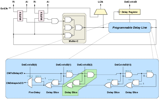
The GALS methodology developed by Muttersbach relies on a pausable local clock generator to prevent metastability during data transfers. Therefore, a fast and reliable local clock generator is the key to a successful GALS implementation. The block diagram of the local clock generator is shown in figure 2.3. The clock generator is basically a ring oscillator whose period can be controlled by programming the delay line. The arbitration block provides the pausability feature to the clock generator.
Figure local_clock_simple
Figure 2.3: Simplified block diagram of a pausable local clock generator.
The local clock generator provides several ports, each of which, when activated, can pause the clock. For each port, the pause request signal (Ri) is combined with the output of the delay line, using a mutual exclusion element (MutEx). MutEx is a specialized circuit that allows only one of its outputs to be at logic-1 at a certain time. There are different implementations of the MutEx. A twelve transistor full-custom implementation that is used for the GALS implementations in the UMC 0.25 m process can be seen in figure 2.4. A rising edge of the local clock can only propagate through the arbitration block if the Ri signals of all ports are logic-0. The output of the arbitration block is combined using a Muller-C gate that essentially only changes its output when both of its inputs are in agreement.
Figure mutex_schFigure mutex_lay
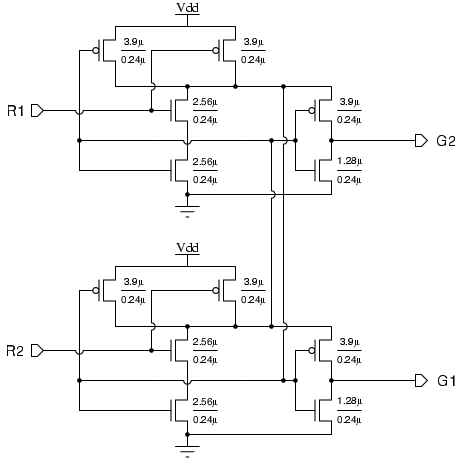
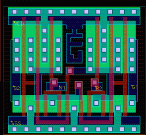
Figure 2.4: The Mutual Exclusion element, transistor schematic (left) and layout (right) for the UMC 0.25  m technology.
As long as one (or more) of the Ri signals is at logic-1, a new clock pulse will not be generated and the local clock will effectively be paused. The next rising edge will propagate through the Muller-C gate only after the blocking Ri signal is returned to logic-0. The MutEx directly generates the clock pause acknowledge signal (Ai) as well. If the Ri request is able to propagate to the Ai output, the clock is effectively paused3. Ai will only return to logic-0 after Ri is lowered.
The number of ports of a pausable local clock generator is not really limited, however combining the outputs of multiple ports reduces the maximum attainable clock frequency somehow. Local clock generators with up to 8 ports have been successfully implemented in practice.
The frequency of the local clock generator can be adjusted using the programmable delay line. However, during normal operation the clock frequency is not changed. The delay line is usually programmed during startup to match the critical path of the module it is connected to. Having a programmable delay line allows the same clock generator to be used for GALS modules with different clock frequencies. Especially for aggressive designs, the exact value of the maximum allowable clock period is not known until the very end of design process. A programmable delay line is practical for such designs as well, since the clock period does not need to be fixed as long as it is within the range of the local clock generator.

2.2.3  Timing Constraints

Depending on the methodology used, several timing assumptions are made during the design phase. As an example, for synchronous designs it is assumed that all inputs of flip-flops are stable before the clock pulse arrives (setup-time constraint) and that they remain stable until the flip-flop has safely sampled its input (hold-time constraint). The circuit will only function correctly if these timing assumptions hold true.
In circuits that use multiple clock domains, this can be tricky, especially on the boundaries between the clock domains. Furthermore, with decreasing feature sizes, an ever increasing portion of the timing is determined by the interconnections. These can only be accurately determined at the final stages of the design, where placement and routing is completed.
The goal of GALS is to handle most of the timing problems that arise in systems with multiple clocking domains, and to impose the least amount of restrictions on the designer of LS islands. To achieve this goal, components of the GALS system must satisfy several timing requirements.
Figure simple_3
Figure 2.5: Two interconnected GALS modules. The latch at the data inputs in GALS module B is required to make sure that the data is still present when the first data edge appears after the data transfer.
The port controllers used in GALS are obtained using asynchronous synthesis tools [CKK+97,YD99a], that convert state transition diagrams into boolean equations. Depending on the specific asynchronous description used, several timing constraints have to be met to ensure proper operation. Similar constraints may exist for the communication between port controllers as well.
The data inputs and outputs are also of concern. Muttersbach strongly advises to use registers at the input and outputs of the LS islands. For synchronous systems, this represents the best case in terms of input and output timing. However, this is not sufficient. Figure 2.5 shows two interconnected GALS modules where the data input of GALS module B is latched by a handshake signal. The latch is only active during the handshake and it stores the data outputs of GALS module A during the data transfer. This is necessary because after the data transfer, LS island A may receive an active clock edge before LS island B. This could change the output of LS island A before LS island B has a chance to sample its inputs 4.
The two control signals Pen and Ta have additional problems. Since Pen is used to activate an AFSM, it must be free of glitches. The easiest method to guarantee this is to use a register for the Pen signal. The Ta signal is used to determine if a pending data transfer has been completed. This signal is required for P-type controllers, where the local clock is only halted during the data transfer. The Ta signal is generated by the port controller and sampled by the LS island. This signal must satisfy several timing constraints to function properly.
Figure timing_channel_wav
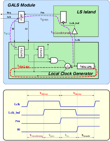
Figure 2.6: Timing constraints of a D-type port. Once activated the port controller must be able to halt the local clock generator before a new clock edge is generated. If the clock tree insertion delay tclocktree is sufficiently large, this timing constraint can not be satisfied.
Specialized port controllers may have additional timing constraints. As an example, Muttersbach presents D-type port controllers that are capable of exchanging data during consecutive clock cycles. As soon as a D-type port is enabled by the Pen signal, it immediately activates Ri to stop the local clock generator. This is shown in figure 2.6. Practically all LS islands need a clock tree to distribute the clock signal. Depending on the size of the LS island, this requires the insertion of several levels of buffers in the clock signal path, resulting in a clock tree insertion delay tclocktree. The clock signal that arrives at the flip-flop generating the Pen signal will be delayed by tclocktree. The flip-flop generating the Pen signal will have a finite propagation delay of tpen and, finally, the Ri signal will be produced with a delay of tri. The sum of all three delays must be less than the nominal period of the local clock generator if the port controller is expected to send data every clock cycle. Aggressive designs may require significant amounts of tclocktree to function properly. The clock tree insertion delay may even exceed the clock period. Other solutions need to be explored for such systems.

2.3  GALS-Based Solutions

The GALS design methodology allows designers to partition a large system into several sub-modules, each of which can be optimized independently. Since the modules do not rely on a global clock to communicate with each other, less effort is required to maintain data integrity on data transfers between modules. Designers using GALS have more freedom to improve the performance of the system. However, this does not imply that simply using GALS will automatically result in a system that is faster, smaller, consumes less power, and is designed in a shorter time.
Most of the GALS systems presented in the literature are based on a working synchronous design. This design is then partitioned into several independent GALS modules in a process that is known as GALSification. Such GALSified systems are at heart still synchronous designs. Several decisions during the design phase of such circuits are based on synchronous constraints. Such systems are less likely to harvest all advantages being offered by GALS, than systems that were from the onset designed with GALS in mind.
The following is a brief discussion of what can be expected by using the GALS methodology for various design parameters:

2.3.1  Low Power

The technological advances in micro-electronic fabrication have enabled the performance of integrated circuits to increase at a rate defined by Moore's Law for the last 4 decades. The factors that resulted in increased performance (smaller transistors, denser circuits, faster switching times) have also increased the amount of power dissipated per unit area. Contemporary high-end micro-processors reach power densities in excess of 100 W/cm2, which is an order of magnitude more than a heating plate used in the kitchen. Therefore reducing the power consumption of digital circuits is of paramount importance.
In a GALS system, modules that are not used frequently can be made to consume less power by either pausing their local clocks until they are needed, or by simply using a reduced local clock frequency (and/or supply voltage) for that particular module. It is also possible to optimize this approach by designing systems that dynamically adjust their frequency and or supply voltage on demand.
Pausing the local clock of a GALS module during times of inactivity is basically equivalent to clock gating at the module level. It can be easily realized by using D-type ports. During a data transfer between GALS modules the local clock will be paused until the interconnected GALS module is ready to send/receive data. While the module is in this 'wait' state, no new clock pulse will be generated, and the module will not consume dynamic power. The power saving that can be achieved by this method depends entirely on how often the module is utilized. Similar gains can also be obtained by using clock gating within the module as well.
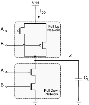
The dynamic power consumption Pdyn of a CMOS circuit is known to be proportional to the activity factor a, the amount of switched capacitance C, the clock frequency f, and to the square of the supply voltage Vdd as given by the well known relation 2.1:

Pdyn » a·C·f·Vdd2
(2.1)
It follows from this relation that, if a module is used less frequently, it is more power efficient to use a lower Vdd which in turn reduces the maximum operating frequency f. So rather than having a fast module (with nominal Vdd) that runs for a short time and then pauses, it is better to use a slow module (with reduced Vdd) that runs at a speed where it does not pause at all. The aim of Dynamic Voltage and Frequency Scaling (DVFS) systems is to achieve this compromise automatically. GALS systems seem to be well suited for implementing DVFS systems since the activity of a module can easily be determined by monitoring the local clock, or the handshake signals. Based on results obtained through simulations, this idea looks promising. In a GALS system specialized for real-time applications, Bhunia et al. [BDBR05] claim up to 67% improvement in throughput per watt over a synchronous implementation.
While the idea seems interesting, there are some problems associated with this approach. Modern devices require very low voltages for power supply around (or even below) 1 V. This does not leave much noise margin for correct operation, and the supply voltage can not be reduced much further to reduce power consumption. Also communication between modules that use different input/output voltages will require level converter circuits.
Early implementations of GALS were based on a premise that using this methodology would result in lower power consumption. While several aspects of the GALS design methodology are in line with practices developed to reduce power consumption, just using GALS does not result in achieving low power designs.

2.3.2  High Performance

The operating frequency of a synchronous system has to accommodate the worst-case propagation delay in the circuit. A self-timed implementation of the same circuit would have a similar performance under the same worst-case condition. However, an optimal self-timed system would be able to finish processing other non-worst-case conditions faster, and consequently, over a large range of samples, it would have an average-case performance that exceeds that of the synchronous system5. For systems where such an average-case performance deviates significantly from worst-case performance (like a ripple-carry adder for instance), self-timed systems can achieve a higher throughput than their synchronous counter-parts. A GALS system may benefit in a similar way as demonstrated by the following hypothetical example:
Assume a system that performs a single operationA, followed by ten operationB. In a synchronous system the slower of both operations would determine the overall clock rate. Let us assume that the critical path of operationA is 3 ns and that of operationB is 2 ns. The synchronous system would require eleven clock cycles of 3 ns totaling 33 ns.
A GALS system that implements each operation as a separate GALS modules would compute operationA within 3 ns and then wait for the result of ten operationB that could be calculated within 20 ns. Communicating between GALS islands adds latency to the system. Even if 3 ns communication overhead is added to the system, the GALS system would be able to complete both operations in 26 ns, more than 20% faster than the synchronous system.
The example given above is overly simplistic and makes several assumptions for a GALS favorable outcome. Nonetheless it demonstrates that under certain conditions GALS systems can indeed increase the throughput, or at least can compensate for the additional latency incurred by communication between GALS modules. A more detailed analysis for a high performance micro-processor architecture is given in [SAM+04].

2.3.3  Ease of Integration

The GALS design methodology allows a very large system to be partitioned into smaller modules, each of which can be optimized independently. At the top level, the designer only has to realize the interconnections between GALS modules which have minor or no timing constraints set on them6. This is in stark contrast to synchronous system-on-chip solutions, where most of the design effort is concentrated to ensure proper distribution of the clock signal and timely arrival of data connections between functional blocks.
In a GALS system, the communication and the functionality are clearly separated. The communication between GALS modules is handled by the asynchronous port controllers, and the functionality is provided by the LS island. The designer of the LS island can therefore focus entirely on the functionality, without worrying about the data communication to other LS islands. In synchronous systems, the sub-blocks typically use the system clock, or derive their own clocks from a central clock, so that inter-block timing constraints can be met. This frequently results in over-constrained sub-blocks, that have to be designed with tighter timing constraints than is really necessary. Moreover, such a sub-block can not always be re-used in a different system, as the timing requirements for this new system may differ from that of the original system. In a GALS system, this is not necessary, the LS island designers are completely free to choose an appropriate local clock rate that fulfills the requirements of the system. The GALS module can be readily re-used since its timing is independent from the environment.
While the goal of earlier GALS implementations centered on improved performance metrics, such as lower power consumption and increased throughput, later publications highlighted the ease of integration as its main advantage.

2.3.4  Secure Applications

In the fourth Workshop on Asynchronous Circuit Design held in June 2004 in Turku, Finland, a special session was held for a joint Strengths Weaknesses Opportunities and Threats (SWOT) analysis for asynchronous circuits. The question that defined the opportunities was:
"Assume you were asking a billion dollars from an investor (to develop self-timed circuits), what would be your strongest argument ?"
Interestingly, cryptographic systems and smart cards was the most commonly stated answer. Practical realizations of cryptographic algorithms in hardware suffer from so-called side channel attacks that can be exploited to compromise the security of the system. Over the years, various publications [SMBY05, TV03, FML+04, YFP03] have claimed that asynchronous circuits are less susceptible to such attacks, mainly since they do not rely on a synchronous clock (a more detailed discussion of this topic can be found in section 3.5.1).
While GALS circuits employ asynchronous communication at the top level, the main functionality is provided by LS islands which are synchronous. Therefore, it may be argued that GALS systems are as susceptible to side channel attacks as their synchronous counterparts. The design presented in chapter 4 is the first application of GALS in a cryptographic system and uses several features of GALS design to improve side channel security.
Cryptographic hardware implementations are in widespread use for more than 30 years. Despite all the effort of the cryptographic community, the threat of side channel attacks against hardware implementations was first discovered in 1996. Evaluating the security of a countermeasure is not trivial. While a novel circuit design method may prove to be effective against a particular side channel attack, it may be vulnerable to other (similar) attacks. It could be argued that, asynchronous circuits, which are not used as widely, have not been scrutinized at the same level as synchronous circuits, which has helped to bolster their reputation of being more 'secure'. The only way to evaluate the security of new ideas, including the GALS-based design presented in this thesis, is to make them available to the cryptographic community for pro-longed analysis.

Chapter 3
Cryptographic Accelerators

3.1   A Cryptology Primer

The word 'cryptology' stems from the Latin word crypto that means 'hiding'. Surprisingly it is mostly associated with secret services, and dark sinister forces that forge evil plans to harm mankind. Throughout history, cryptology was mostly used to protect secrets. With the advent of the digital age, cryptology has transformed itself from a science that is used by the military and intelligence services to an essential part of the the digital information society.
Storing information digitally has many advantages. A digital content can (at least theoretically) be stored without loss or degradation indefinitely7. Not only that, but it can be copied, duplicated and transferred electronically with ease. Today, all sorts of information from simple letters to books, pictures, movies, medical records and business transactions are stored and transferred electronically in digital form.
Despite these advantages, there are some important problems associated with digital content. It can be changed at any time, without leaving a single trace. After all, it is not even possible to tell who has created a given digital information. Businesses that rely on distribution of information (news, music and media industry) do not take it too kindly that their revenue generating digital information can be copied freely either.
It is only with the help of cryptology that the above mentioned problems can be reliably addressed. The following is a list of some essential security services that are required in a working digital society.
Confidentiality:
The content of the information is kept secret. This is the basic service that is most commonly associated with cryptology.
Integrity:
The information has not been modified.
Authenticity:
The author (origin) of the information is known.
Access Control:
Access to information is restricted to certain users.
Non Repudiation:
The author of an information can not deny creating the information. This is important for digital transactions. Imagine a scenario where Alice places an order electronically. Once the order is completed, Alice should not be able to claim that she did not place the original order.
The branch of cryptology that is dedicated to develop methods that provide these services is called 'cryptography'. and systems providing these services are called cryptographic systems. The key part of a cryptographic system is a cryptographic algorithm that essentially provides a method to transform legible information (plaintext) into a form that is protected (ciphertext) with the help of a secret information (cipherkey).
The simple model given in figure 3.1 describes key components of a cryptographic algorithm. It has become common to personify the users of cryptographic systems 8. Alice and Bob are users of the crypto system and have access to a secret cipherkey. Oscar represents the malicious attacker who does not have access to the cipherkey, but is generally assumed to have unlimited access to the ciphertext. The process of transforming plaintext into ciphertext is known as encryption and the reverse process is known as decryption. The security of a cryptographic algorithm is defined by the difficulty in which the plaintext can be obtained from the ciphertext without knowing the cipherkey, a process known as 'breaking a cryptographic algorithm'. A second branch of cryptology, called cryptanalysis, concentrates on finding weaknesses of cryptographic algorithms and thus contributes to development of better (more resistant) algorithms.
Figure alice_bob
Figure 3.1: Simple model for cryptographic algorithms.
Designing cryptographic algorithms is a challenging process. The ultimate goal of such an algorithm is to achieve 'unconditional security'. An unconditionally secure algorithm can not be broken even with infinite amount of computation resources. Unfortunately, the practical realization of such algorithms have proven to be difficult9. What is more frequently used are 'computationally secure' algorithms. Breaking these algorithms requires a very large amount of computational resources. As long as the effort required to break the algorithm is sufficiently high10, the algorithm is considered to be secure. Most algorithms rely on well studied mathematical problems considered to be difficult to solve. There is, however, no proof that these problems can not be solved faster, because scientists were simply unable to do so over a long period of time. Cryptographers live in constant fear of a discovery that provides a faster solution to a mathematical problem serving as a foundation of their algorithm. This is the main reason that most modern cryptographic algorithms are required to go through a public review process.
Depending on how the cipherkey is managed, the cryptographic algorithms can be classified into publickey algorithms and privatekey algorithms. Publickey algorithms use a cipherkey that consists of two parts. Bob makes the public part of the cipherkey known to the whole world, and keeps the second part secret. When Alice wants to send a message to Bob, she uses this public key to encrypt the message. The public key algorithms are designed in a way to enable a decryption of the ciphertext only with the second (secret) part of the cipherkey. RSA [RSA78] is probably the best known publickey algorithm used today. Privatekey algorithms, on the other hand, rely on a cipherkey that both Alice and Bob know and keep secret.
Publickey algorithms are usually computationally intensive and are therefore not suited for secure transmission of lengthy messages. Privatekey algorithms are suited for bulk transmission, but it is a challenge to distribute the required secret cipherkey. Typical secure applications on the Internet use a public key algorithm to negotiate a sessionkey between Alice and Bob. This sessionkey is then used as the cipherkey of a privatekey algorithm to transfer data between Alice and Bob.
Privatekey cryptographic algorithms that use the same cipherkey to process multiple plaintext ciphertext pairs are called block ciphers. Common cryptographic algorithms like DES [Nat99] and its successor AES [Nat01a] fall into this category.

3.2   Advanced Encryption Standard (AES)

The first algorithm that was widely used in public is the Digital Encryption Standard (DES) algorithm that has been introduced as a U.S. federal standard in 1976. DES is a block cipher that operates on 64-bit words and uses a 56-bit cipherkey. DES (with its variations) was widely used for more than 20 years.
The main problem of the DES algorithm was its relatively short cipherkey, with 256 possible keys. Although this a fairly large number (72,057,594,037,927,936), with sufficient computational resources brute force attacks on DES are feasible. So-called DES challenges, where a large number of computers connected to the Internet exhaustively searched the key space, demonstrated this weakness dramatically. The first DES challenge in 1997 was completed in 4.5 months, the second in 1998 in 39 days and the third and final DES challenge in 1999 was completed in less than a day (22.5 hours) 11.
In 1997 the US National Institute of Standards and Technology (NIST) started a public competition to select an algorithm to replace DES. The algorithm was required to be a block cipher supporting cipherkey lengths of 128, 192, and 256 and to be free of any patents. The selection process consisted of several rounds where candidate algorithms were evaluated. At the end of the first round in August 1998, 15 algorithms were accepted as candidates. In the next round in August 1999, the candidates were reduced to five finalist algorithms (MARS, Blowfish, RC6, Rijndael, Serpent). Finally, in April 2000 the Rijndael algorithm was selected as the winner. On 2 October, 2000, NIST officially announced that Rijndael has been chosen as Advanced Encryption Standard (AES).
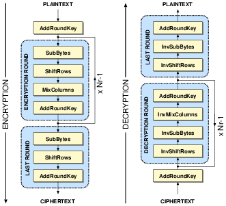
The AES algorithm is a block-cipher operating on 128-bit data blocks12 supporting three different cipherkey lengths of 128, 192 and 256 bits. These three flavors of the AES algorithm are also referred to as AES-128, AES-192 and AES-256, for 128, 192, and 256-bit cipherkeys, respectively. An AES encryption process consists of a number of encryption rounds (Nr) that depends on the length of the cipherkey. The standard calls for 10 rounds for AES-128, 12 rounds for a AES-192, and 14 rounds for a AES-256. During encryption, each round is composed of a set of four basic operations. The decryption process applies the inverse of these operations in reverse order. Figure 3.2 shows the basic structure of the AES encryption and decryption.
Figure aes
Figure 3.2: Basic structure of the AES algorithm: encryption (left), decryption (right).

3.3   AES operations

Figure state
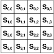
Figure 3.3: In AES, 128-bit data is represented as a four-by-four byte matrix called state.
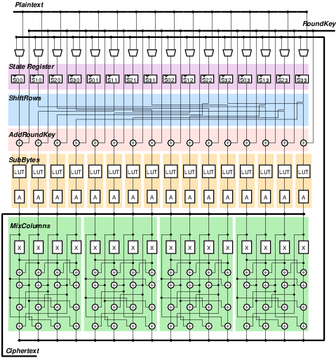
In the AES standard [Nat01a], the 'state' is defined as a byte matrix consisting of four rows and four columns as shown in figure 3.3. The element Sr,c is a 8-bit value that corresponds to the row r and column c of the state. A typical AES implementation uses a 128-bit state register as part of the round architecture. The operations that make up the AES algorithm are defined as operations that modify the state. The following subsections explain all operations in detail and provide a discussion on their implementations in hardware. All operations (except AddRoundKey, which is its own inverse) have a similar inverse operation. For clarity purposes, the text will refer to only the 'forward' operations in general descriptions. A block diagram of a complete AES encryption datapath is given in figure 3.4 for reference.
Figure aes_enc
Figure 3.4: Block diagram corresponding to a parallel 128-bit encryption only realization of AES as shown in figure 3.2. All operators and thin data connections are 8-bit and the thick lines represent 128-bit busses. (A) is the affine transformation and (X) is the xtime function.

3.3.1  AddRoundKey

During each round of an AES process, a separate 128-bit roundkey is used. The roundkeys are derived from the cipherkey using a key expansion routine. The AddRoundKey operation is a simple bit-by-bit XOR operation between the state and the roundkey. An AES process requires a total of Nr+1 AddRoundKey operations, as an additional 'initial' AddRoundKey operation is performed prior to the round operations. For an AES encryption process this initial AddRoundKey operation XORs the plaintext with the cipherkey. Since XOR is an involutory operation, AddRoundKey is used during the AES decryption process as well.
There is little that can be done in a hardware implementation to optimize the AddRoundKey operation, as it consists solely of XOR gates. Attempts to reduce the number of parallel XOR gates often require multiplexer structures that have an area overhead comparable to the area saved.
There is a need for an additional AddRoundKey operation during an AES process, as there are Nr rounds and Nr+1 subkeys. For most cases it is more efficient to implement a separate AddRoundKey function block in hardware for this additional operation than to share one block for all AddRoundKey operations.

3.3.2   SubBytes and InvSubBytes

Cryptographic algorithms require non-linear operations to be successful. SubBytes is the primary non-linear operation of the AES algorithm. It is an 8-bit transformation applied to each byte of the state independently. It consists of two separate transformations:
  1. The multiplicative inverse of each state byte in the finite field GF(28) is taken13. The hexadecimal value 0x00 is mapped on to itself.
  2. The affine transformation over GF(28) described by the following pseudo-code:

    -- Affine transformation in AES
    -- S(i) is the ith bit of the 8-bit input
    -- Z(i) is the ith bit of the 8-bit output
     
    Z(0) <= S(0) xor S(4) xor S(5) xor S(6) xor S(7) xor '0';
    Z(1) <= S(0) xor S(1) xor S(5) xor S(6) xor S(7) xor '1';
    Z(2) <= S(0) xor S(1) xor S(2) xor S(6) xor S(7) xor '1';
    Z(3) <= S(0) xor S(1) xor S(2) xor S(3) xor S(7) xor '0';
    Z(4) <= S(0) xor S(1) xor S(2) xor S(3) xor S(4) xor '0';
    Z(5) <= S(1) xor S(2) xor S(3) xor S(4) xor S(5) xor '0';
    Z(6) <= S(2) xor S(3) xor S(4) xor S(5) xor S(6) xor '1';
    Z(7) <= S(3) xor S(4) xor S(5) xor S(6) xor S(7) xor '1';

During a decryption process the InvSubBytes operation is used. It is similar in nature to the SubBytes operation and consists of the following two steps:
  1. The inverse affine transformation over GF(28) described by the following pseudo-code:

    -- Inverse Affine transformation in AES
    -- S(i) is the ith bit of the 8-bit input
    -- Z(i) is the ith bit of the 8-bit output
      
    Z(0) <= S(2) xor S(5) xor S(7) xor '0';
    Z(1) <= S(0) xor S(3) xor S(6) xor '1';
    Z(2) <= S(1) xor S(4) xor S(7) xor '1';
    Z(3) <= S(0) xor S(2) xor S(5) xor '0';
    Z(4) <= S(1) xor S(3) xor S(6) xor '0';
    Z(5) <= S(2) xor S(4) xor S(7) xor '0';
    Z(6) <= S(0) xor S(3) xor S(5) xor '1';
    Z(7) <= S(1) xor S(4) xor S(6) xor '1';

  2. The same multiplicative inverse for GF(28) that was used for SubBytes.
The performance of an AES chip depends mainly on the implementation of the SubBytes function. There are basically two main implementation choices for hardware: using a look-up table or applying arithmetic decomposition.
SubBytes is a 8-bit function. A look-up table that implements SubBytes contains 256 entries that are 8-bit wide. A mask ROM would be most suited for this purpose. However, ROM generators are technology dependent and are sometimes not directly available for a given technology. Full custom design is another alternative, but is a time-consuming process. A common, technology independent method is to map the look-up table to standard cells using a synthesis tool like the Synopsys design_analyzer.
Most modern FPGA architectures contain dedicated RAM arrays. AES implementations on FPGA's frequently make use of these RAM arrays by initializing them with the look-up table contents [MM03].
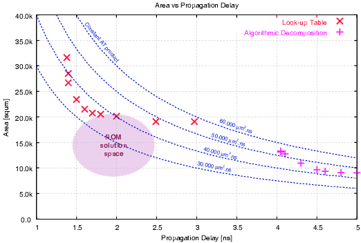
The second approach would be to find an algorithmic way to compute the SubBytes function. The main difficulty in this is the multiplicative inverse in GF(28) which requires excessive calculation and circuit area. However, an operation in GF(28) can be decomposed into operations in GF(24) as reported by Wolkerstorfer et al. [WOL02]. Figure 3.5 compares this approach to the synthesized look-up table. The multi-level architecture of the algorithmic decomposition results in a high propagation delay, compensated by the much smaller area. Overall, it can be clearly seen that both implementations share a common AT product. Figure 3.5 also contains the expected solution space for a mask ROM solution 14.
Figure sbox3
Figure 3.5: 8-bit SubBytes implementations in 0.25 m CMOS technology. A ROM generator does not exist for this particular technology. The figures for ROM have been obtained by full-custom design of SubBytes.
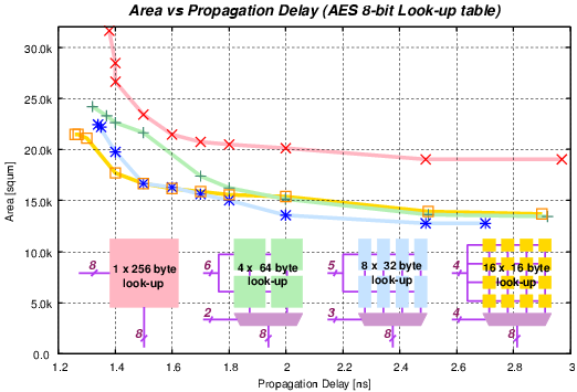
Traditional logic synthesis programs have difficulties in processing large look-up tables. Better results can be obtained by partitioning the look-up table into smaller ones. Figure 3.6 compares the circuit area and propagation delay of four different SubBytes implementations. Instead of using a single look-up table with 256 entries, the use of 8 look-up tables each with 32 entries can reduce the area by almost 30%. Experience has shown that the synthesized look-up tables result in netlists that require noticeably high routing overhead. It is difficult to quantify this overhead, as it is technology and library dependent, but it can result in noticeably larger circuits after the placement and routing phase.
Figure sbox2_4
Figure 3.6: Decomposing the look-up table for SubBytes can lead to more efficient implementations.

3.3.3  ShiftRows and InvShiftRows

The ShiftRows operation changes the order of bytes in each row of the state. The first row is not affected by this transformation. The second row is shifted cyclically to left by one byte, the third row by two and the fourth row by three bytes as seen in figure 3.7. The inverse operation InvShiftRows is quite similar in style, with only the cyclic shifts made to the right.
Figure ShiftRows
Figure 3.7: ShiftRows and InvShiftRows transformations. Shaded bytes are wrapped around as a result of the cyclic shift operations.
In a 128-bit parallel implementation of AES, ShiftRows can be implemented by wiring between operations without any hardware resources15. However, implementations that process fewer than 128-bits per clock cycle face a data-dependency problem. If no precautions are taken, the output of the first MixColumns operation following ShiftRows will replace unprocessed values in the state register. An obvious solution is to use an additional 128-bit round register. Depending on the round architecture, the amount of additional flip-flops can be reduced by clever scheduling of operations. However such elaborate organizations rely on selection circuitry, with additional area and propagation delay penalties.

3.3.4   MixColumns and InvMixColumns

MixColumns is a 32-bit operation that transforms four bytes of each column in the state. The new bytes of the column S¢r,c are obtained by the given constant matrix multiplication in GF(28). If the polynomial representation of binary numbers are used, this multiplication can be given as

é
ê
ê
ê
ê
ê
ë
S¢0,c
S¢1,c
S¢2,c
S¢3,c
ù
ú
ú
ú
ú
ú
û
=
é
ê
ê
ê
ê
ê
ë
x
x+1
1
1
1
x
x+1
1
1
1
x
x+1
x+1
1
1
x
ù
ú
ú
ú
ú
ú
û
· é
ê
ê
ê
ê
ê
ë
S0,c
S1,c
S2,c
S3,c
ù
ú
ú
ú
ú
ú
û
(3.1)
The addition in GF(28) is performed by the XOR operation. Multiplication on the other hand is more involved. A practical xtime function is defined for multiplication with x in GF(28). This xtime function can be described in the following pseudo-code:

-- xtime function
-- S(i) is the ith bit of the 8-bit input
-- Temp(i) is the ith bit of an 8-bit intermediate value
-- Z(i) is the ith bit of the 8-bit output
 
Temp(7 downto 0) <= S(6 downto 0) & '0';
 
if (S(7) = '1') then 
 Z <= Temp xor "00011011";
else
 Z <= Temp;
end if;

The Inverse function InvMixColumns is similar but requires a more complicated matrix multiplication:

é
ê
ê
ê
ê
ê
ë
S¢0,c
S¢1,c
S¢2,c
S¢3,c
ù
ú
ú
ú
ú
ú
û
=
é
ê
ê
ê
ê
ê
ë
x3+x2+x
x3+x+x
x3+x2+1
x3+1
x3+1
x3+x2+x
x3+x+x
x3+x2+1
x3+x2+1
x3+1
x3+x2+x
x3+x+x
x3+x+x
x3+x2+1
x3+1
x3+x2+x
ù
ú
ú
ú
ú
ú
û
· é
ê
ê
ê
ê
ê
ë
S0,c
S1,c
S2,c
S3,c
ù
ú
ú
ú
ú
ú
û
(3.2)
To obtain higher powers of x, the xtime function can be used repeatedly.
It is apparent from equations 3.1 and 3.2 that the InvMixColumns operation is more involved than that of MixColumns. Since all other operations in an AES round are more or less balanced in terms of both area and propagation delay, the difference in implementing MixColumns and InvMixColumns is directly reflected in the overall AES encryption and decryption performance. In a cryptographic system where a data stream is processed, the overall system speed is determined by the slowest of the encryption and decryption operations. In [GBG+04], this problem is examined in detail and a balanced architecture for both encryption and decryption is presented. This is obtained by optimizing the decryption path that includes the InvMixColumns operation aggressively to match the propagation delay of the encryption path. In terms of hardware complexity, the MixColumns operation can be mapped to a couple of stages of XOR gates and ends up requiring roughly 2-4 times more gate area than that required by the AddRoundKey function.
In the AES standard, the last encryption round does not require a MixColumns operation and similarly the last decryption does not require an InvMixColumns operation. Apparently this was made to allow a symmetric encryption and decryption flow. Hardware implementations hardly profit from this arrangement. Especially high-performance implementations suffer from additional hardware overhead to treat the last round differently.

3.3.5   Key Expansion

The key expansion routine is used to generate the roundkeys from the cipherkey. The AES standard defines the key expansion operations on four byte words called wi. A subkey is composed of four such words. The key expansion for AES-128 is relatively straightforward:
Unfortunately, the key expansion routine for other cipher key lengths introduces more irregularity to this basic process (see [Nat01a] for details). Implementations that support multiple cipher key lengths suffer excessively from this problem. Although the key expansion routine contains much less hardware than a regular AES round, the critical path of the AES system is more often located within the key expansion routine as a result of the flexibility required to implement different key lengths.

3.4   AES Hardware Implementations

Cryptographic algorithms are computationally demanding algorithms. Even powerful 64-bit micro-processors require hundreds of clock cycles to en/decrypt AES, which can be considered relatively software friendly. Public key algorithms like RSA may require as many as a million clock cycles on the same processor. The throughput of a cryptographic system is relevant when a continuous stream of data, such as video and audio streams are processed16. Such data streams may require processing rates from few Kbit/s to hundreds of Mbit/s. Especially for systems that require continuous execution of cryptographic operations, designing custom hardware to accelerate cryptographic operations is an efficient alternative to using general purpose micro-controllers.
Early stages of the AES evaluation process required "computationally efficient" implementations. Most algorithms developed for AES were primarily optimized for a Pentium system. Eventually, in the later stages of the evaluation, the candidate algorithms were also compared in terms of their suitability for hardware implementation. Several early papers [IKM00, WBRF00] provided a general overview without algorithm specific optimizations. In [LTG+02] two of the finalist algorithms (Serpent and Rijndael) were actually implemented in hardware.
After Rijndael was selected to be the AES standard, a relatively large number of AES hardware implementations were presented [VSK03, GBG+04, SMTM01, LT02, SLHW03, KMB03]. As described previously in section 3.3, AES consists of few simple hardware operations. The main factors determining the design of an AES hardware are described in more detail below.

3.4.1  Datapath Width

For a 128-bit parallel AES implementation as much as 80% of the area and more than 50% of the propagation delay is contributed by SubBytes, and the datapath width is practically determined by the number of parallel SubBytes operations performed in one clock cycle. Since 128 bits of data need to be processed during each AES round, the number of parallel SubBytes operation also directly determines the number of clock cycles required for an AES process. This represents a direct tradeoff between throughput and circuit area.
As described earlier, the ShiftRows operation can be realized without any special hardware resources for a 128-bit parallel implementation. However, AES datapaths that process less than 128 bits per clock cycle may be forced to either add additional intermediate registers or use extra clock cycles to overcome data dependency problems between ShiftRows and MixColumns.
In table 3.1, synthesis results from five AES encryption datapaths with different datapath widths are given for comparison. While smaller datapath widths result in a small architecture, they require additional selection circuitry between AES operators. This adds to the critical path, and increases the area.
Datapath Width8-bit16-bit32-bit64-bit128-bit
Parallel SubBytes units124816
Complexity (gate equivalents)5,0526,2817,15511,62820,410
Area (normalized)11.2661.4722.4324.269
Clock cycles for AES-12816080402010
Critical Path (normalized)1.3491.3411.2061.1331
Total time for AES-128 (normalized)21.58010.7294.8252.2271
Table 3.1: Synthesis results for five different datapath widths of a simplified AES encryption datapath. The additional hardware resources for ShiftRows have not been taken into account in this analysis.

3.4.2  Encryption/Decryption

One of the essential questions when designing custom AES hardware is whether or not the inverse AES process (AES decryption) is going to be supported. The NIST standard defines five operation modes for AES [Nat01b]:
Of these five modes, only ECB and CBC require the inverse AES operation for decryption. All other modes use a stream of AES encryptions to generate a pseudo-random sequence that are used to encrypt the plaintext. The decryption process for these modes requires exactly the same pseudo-random sequence that is generated by using the same stream of AES encryptions. Therefore, there are some systems where AES decryptions are not required at all.
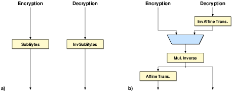
Figure invsbox
Figure 3.8: Two alternative realizations for implementing SubBytes and
InvSubBytes.
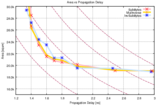
As the AES encryption and decryption processes are very similar to each other, a datapath that implements both functions is conceivable. The main problem in such an implementation is once again the SubBytes function. The inverse function InvSubBytes is equally complex and requires significant resources. Rather than using two separate functions as seen in figure 3.8a, both functions can be realized by sharing the multiplicative inverse. The resulting datapath will resemble the one shown in figure 3.8. When implemented as a synthesized look-up table all three functions (SubBytes, InvSubBytes, Multiplicative Inverse) require identical hardware resources (figure 3.9). The shared datapath as shown in figure 3.8b will result in a longer critical path due to additional transformations and selection circuitry. Designs targeting high throughput rates will often use a structure that supports only encryption or will employ separate datapaths for encryption and decryption.
Figure sbox1
Figure 3.9: Comparison of look-up tables implementing SubBytes, InvSubBytes and multiplicative inverse in GF(28). Synthesis results for 0.25 m CMOS technology.

3.4.3   The AES Round Organization

The goal of a hardware designer implementing AES is to come up with a datapath that implements the AES round efficiently. Such a round would generally contain one register for the state. Although the structure of the AES round has been defined in the standard for encryption and decryption, it is possible to re-order operations without changing the result.
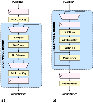
Figure 3.10 shows two possible organizations for the AES encryption round. A straightforward implementation of the algorithm (similar to figure 3.3) is given in figure 3.10a. The multiplexer between MixColumns and AddRoundKey is necessary for the last round of the encryption where the MixColumns operation is not executed. This multiplexer remains in the critical path throughout the entire operation. By re-ordering the operations, this multiplexer can be removed entirely from the hardware architecture. The ShiftRows operation is independent from both SubBytes and AddRoundKey and can be moved to a convenient location. The output is obtained by tapping into the hardware round after the SubBytes operation. In this organization, the additional AddRoundKey operation is executed separately at the end. This is not very costly, since AddRoundKey is the AES function with the least penalties for area and propagation delay. This architecture can be seen in figure 3.10b.
Figure reorder
Figure 3.10: Two different architectures for the AES encryption datapath: a) one to one implementation of the standard, b) re-ordered round structure with the additional AddRoundKey at the end.
A similar organization is made in [LTG+02] to insert a pipeline register into a datapath that supports both encryption and decryption. Separate organizations are used for encryption and decryption to find a suitable location to insert an additional pipeline register. Note that inserting pipeline registers may improve the clock rate of the system, but a higher throughput can only be obtained if independent data blocks are processed at the same time. Unfortunately, only ECB and CTR modes of operation can be used in such a pipelined system17.

3.4.4   Roundkey Generation

There are two main approaches to generate the roundkey used in the AES process. Keys can be generated on-the-fly by a concurrently executing datapath that computes the next roundkey during the time the actual datapath completes computing the current AES round. The second alternative is to pre-compute all roundkeys and store them in a roundkey memory.
A critical point in the implementation of a cryptographic system is the "key setup time" which is defined as the amount of time required to start cryptographic operations after a new cipherkey has been provided. On-the-fly key generators can be designed in a way to completely eliminate any latency overhead when changing cipherkeys, at least for encryption. For decryption, the first roundkey that is required is the last roundkey that has been used for encryption. Since the key expansion uses recursion, there is no simple way to obtain the last roundkey directly from the cipherkey. This must be done by computing all roundkeys for the encryption. The last roundkey so obtained can be used as an initial vector for the inverse key schedule.
The AES-256 mode requires 15 roundkeys with 128 bits. An on-the-fly key generator of a flexible AES implementation that supports both encryption and decryption for all standard key lengths needs to be able to store 256 bits of cipherkey, 128 bits for the roundkey, and finally 128 bits for the last roundkey. This is more than one fourth of the total amount of storage that is needed for all roundkeys. Consequently, pre-computing all roundkeys is not always a bad decision.
At first sight, the key expansion defined for AES (section 3.3.5) does not look hardware intensive. After all, only four SubBytes operations are required per AES round. However, the additional flexibility required to support all three key lengths results in a very cumbersome and slow implementation. For faster implementations with large parallel datapaths, the critical path through the key generator is usually longer than the actual datapath. For small implementations that use a datapath of 32 bits or less, more area is required to implement a key generator than the actual datapath.

3.4.5  Comparison of AES chips

There are many reported hardware implementations of AES in literature. Table offers a comparison of the key properties of these implementations. Ichikawa et al. [IKM00] presented a comparison of all AES candidates in hardware during the AES evaluation process. This early evaluation is not very representative, as no optimizations of any sort were made. The very large reported area is a result of a completely unrolled architecture for 10 hardware rounds. The reported throughput figure is a result of pipelining and only achievable in the ECB mode.
The implementations reported in [VSK03] and [KMB03] are high-speed designs that support three plaintext block sizes of 128, 192 and 256 bits as described in the original Rijndael specification. The additional block sizes, which are not part of the AES standard, add to the complexity. Both designs are capable of delivering higher throughput for these modes.
The SubBytes function has been implemented by using masked ROMs in [KMB03]. The high throughput reported by [SLHW03] is achieved by pipelining, which can not be used in feedback modes. This chip uses an algorithmic decomposition to implement the SubBytes function. Three of the four pipeline stages used in the round are dedicated to implementing the SubBytes function.
The design in [LT02] shares major datapath components between encryption and decryption. The SubBytes and its inverse is performed by using a single look-up table for the multiplicative inverse. A range of architectures with different datapath widths are presented in [SMTM01]. Unfortunately none of the architectures was implemented in silicon, and the presented results are from synthesis runs. While synthesis results certainly contain useful information and can be reliably used to compare different approaches, we have found it difficult to replicate the same performance obtained during synthesis after physical design. Most of the approaches and optimizations require large data buses with 128 bits or more to be distributed, and require significant amounts of selection circuitry, all of which are challenging tasks in the back-end design flow. Furthermore, look-up tables often employed in AES have very high demands on placement and routing. Some designs also use high clock rates and employ a large number of flip-flops, which results in severe clock distribution problems.
Verbauwhede
[VSK03]
Kim
[KMB03]
Satoh
[SMTM01]
Su
[SLHW03]
Lu
[LT02]
Ichikawa
[IKM00]
Technology0.18 m0.18 m0.11 m0.25 m0.25 m0.35 m
Area3.96 mm2N/A0.205 mm21.62 mm2N/AN/A
Gate Equivalents173,00028,62621,33763,40031,957612,834
RAM-4Kb-4Kb--
ROM-128Kb----
Throughput1600 Mb/s1640 Mb/s2600 Mb/s2970 Mb/s610 Mb/s1950 Mb/s
En/Decryptionencryptionboth/sharedbothbothboth/sharedboth
ModesallECBECB/CBCECBECBECB
Key Generationon-the-flystoredon-the-flystoredon-the-flystored
Key Lengths128/192/256128/192/256128128/192/256128128
Datapath256-bit256-bit128-bit128-bit128-bit128-bit
Notessupports 256-bit datasupports 256-bit datasynthesis results pipelinedsynthesis results unrolled rounds
synthesis results
Table 3.2: Comparison of AES implementations reported in literature.
A total of six different AES implementations in silicon have been designed at the IIS. A comparison of these architectures is listed in table . The first chip Riddler was designed by Adrian Lutz, Andres Erni and Stefan Reichmuth, as part of their semester thesis during the winter semester of 2001/2002. The goal of the semester thesis was to compare the two leading AES candidates Rijndael and Serpent with an emphasis on throughput. The students were in direct competition with a second group of students (Jürg Treichler, Gerard Basler and Pieter Rommens) that implemented the Serpent algorithm. The results were surprising [LTG+02]: both chips designed by teams with similar design experience within the same time, occupying exactly the same area (49 mm2 including pads in a 0.6 m CMOS technology) had almost the same measured throughput (around 2 Gb/s). Riddler uses two identical 128-bit AES rounds in parallel. The throughput figure is therefore only attainable for ECB and CTR modes of operation. The round structure uses a common multiplicative inverse look-up table, similar to the configuration shown in figure 3.8. The roundkeys are pre-computed and are stored in a register array.
Fastcore was designed by Franco Hug and Dominique Gasser during the 2002/2003 winter semester. The goal in this design was to support all operation modes and key lengths, and to obtain the highest possible throughput within a pre-determined core area (3.56 mm2 in a 0.25 m CMOS technology). The design has separate 128-bit encryption and decryption datapaths each with an independent on-the-fly key generator. As reported in [GBG+04] the design was optimized to have a balanced throughput for both decryption and encryption.
Riddler [LTG+02]Fastcore [GBG+04]Ares [PGH+04]BabyPampersAcacia
Technology0.6 m0.25 m0.25 m0.25 m0.25 m0.25 m
Area37.8 mm23.56 mm21.2 mm20.35 mm20.58 mm21.1 mm2
Gate Equivalents75,000119,00042,40814,25923,07639,012
RAM-----2Kb
ROM------
Throughput2160 Mb/s2120 Mb/s1150 Mb/s285 Mb/s230 Mb/s180 Mb/s
En/Decryptionboth/sharedconcurrentencryptionencryptionencryptionboth/shared
ModesECBallECB/OFBECB/OFBECB/OFBECB
Key Generationstoredon-the-flyon-the-flyon-the-flyon-the-flystored
Key Lengths128128/192/256128128/192/256128/192/256128/192/256
Datapath2 x 128-bit128-bit128-bit16-bit16-bit2 x 16-bit
Table 3.3: Comparison of AES implementations fabricated at the IIS.
During the summer of 2003, using a differential power analysis (DPA) attack, parts of the cipherkey were successfully recovered from a Fastcore chip [OGOP04]. This is the first reported successful DPA attack on an ASIC implementing the AES algorithm. The experience obtained from this attack has resulted in a string of AES designs that include countermeasures against DPA attacks. In his diploma thesis, Norbert Pramstaller investigated algorithmic countermeasures against DPA attacks[PGH+04]. The Ares chip was designed as part of this thesis during the winter semester of 2003/2004. The chip includes a 128-bit datapath and a separate (more flexible) 32-bit datapath both of which that support only 128-bit encryption. The numbers presented in table 3.3 are from the 128-bit core.
While all these chips were designed with primarily high throughput in mind, the Baby chip, by Peter Haldi and Stefan Zwicky during the 2004/2005 winter semester, was designed as a small and efficient AES implementation. This chip serves as a reference design for the Pampers chip that includes delay- and noise-based countermeasures against DPA. Pampers was developed by Stefan Achleitner as part of his diploma thesis during the 2004/2005 winter semester in parallel with Baby. Both designs use a dedicated key generator that supports all key lengths. Finally, Acacia, which will be explained in detail in chapter 4, is a GALS-based DPA-resistant AES implementation.

3.5  Cryptographic Security

As mentioned earlier in section 3.1, cryptographic systems are used to provide various security services. To illustrate the problems associated with these services let us consider the following smart card system used in private banking18. As part of a general strategy to increase customer satisfaction and reduce personnel costs, banks hand out so-called smart cards to account holders (users). By using Automated Teller Machines (ATM) that are located at convenient locations, the users are able to access a large portion of the bank services any time. Even in this relatively simple system different security aspects can be observed.
  1. Alice, who has an account at the bank, has an interest in protecting her bank account from others. The bank is primarily used as a safe place to deposit cash after all. Alice wants to be sure that only she is able to determine how money can be withdrawn from her account. Much like a regular house key, physical possession of the smart card is the primary method in which Alice is able to access her account.
  2. Oscar, who lives in the same fictional city as Alice, is a person with malicious intent. He is an expert in electronics, is extremely patient, and will consider all alternatives short of an armed robbery to get rich by manipulating bank services. He also knows all there is to know about the computing system of the bank.
  3. Alice is worried that, if she accidentally misplaces her smart card, Oscar could find it before her and instead of returning the smart card to her, he might decide to withdraw money from her bank account. The bank decides to implement a security system to comfort Alice. She is able to determine a password that is stored on the smart card. To access her bank account, Alice must use her smart card and correctly type in the password before using the ATM.
  4. Both the bank and Alice are worried about the fact that the communication from the ATM to the bank computer can be observed or even altered by Oscar. Therefore, the data transmission that contains the instructions from Alice to the bank, and information relayed back to Alice by the bank are encrypted. This sort of encryption needs a secret key that is known to both Alice and the bank.
  5. Since there are many similar account holders like Alice, the bank decides that it is more efficient to use the same secret key for all account holders. While the bank enjoys having Alice as a customer, it also does not want to entrust the secret to Alice directly. This is understandable, because Oscar might simply pose as an innocent customer, open a bank account at the same bank. By doing so he would receive a smart card himself and would automatically be given the same secret key. Oscar could then use his skill in wire tapping, to create mischief while Alice is using the system. As a solution, the bank decides to engrave the secret key into the smart card. Oscar can still obtain a smart card and try extracting the secret key, but the bank is convinced that Oscar will fail in all attempts in doing so.
  6. The ATM is another source of worry for both Alice and the Bank. Oscar has been known to place his own 'evil' ATMs that masquerade as the original 'good' ATMs. Alice does not trust any ATMs, as she does not know how to tell apart good and evil ATMs. The bank, afraid of losing good customers, adds another feature to its electronic banking system. Before the smart card exchanges any vital information with the ATM, it puts the ATM to a test. The smart card poses a question that can only be answered with explicit knowledge of the secret key. The evil machines prepared by Oscar would not know this secret. After all it is the desire to reveal this secret that drives Oscar to place these machines in the first place.
The first observation from this scenario is that a secure information system consists of several methods that are used in combination. The security of the overall system depends on the security of individual components. What is not discussed here, but is just as relevant, is the social side of the secure systems (see [And93] for some examples). For it is also possible to imagine Oscar trying to bribe, extort or somehow obtain the cooperation of bank employees.
When considering attacks on cryptographic systems, Oscar is assumed to have full knowledge of the entire system, but is considered not to posses any prior information on the secret key (Kerkhoffs Principle). The security of the system is defined by the effort that is required on part of Oscar to reveal the secret key. This directly defines the cost of breaking the system. A successful system is one where the benefits obtained by breaking the system is far less than the cost of performing such an attack.
The fact that Alice and Bob share a mutual secret (knowledge of the key), and their desire to exchange information, does not necessarily mean that they 'trust' each other. In the example above, the bank (imagine for arguments sake that the computer system of the bank is Bob) is not able to distinguish Alice from Oscar directly. Therefore the bank treats all its customers as a potential Oscar.
One of the main challenges in building a secure system is to find an adequate method of distributing the secret key used in various algorithms of the system. From a security point of view, it is desirable to use a different secret key for each user or even for each transaction of each user. This is however not always feasible. There are many instances, like the simplified smart card example above, where a secret key is embedded in a device that is available to all users of the system, including potential malicious users like Oscar.

3.5.1   Side Channel Attacks

Good cryptographic algorithms (like the AES algorithm presented in section 3.2) are designed to make it practically impossible to extract the cipher key by observing the outputs (known ciphertext attacks), or by providing specific inputs (chosen plaintext attacks). At least, the security in terms of the effort required by Oscar to perform a successful attack is well known and is deemed adequate for specific applications.
The implementation of a cryptographic algorithm results in a black box that has several observable physical properties such as power consumption, electromagnetic radiation, surface temperature, time required to complete an operation, or even sounds generated by this black box. All these properties that can be observed to change while cryptographic operations are processed, are information sources which can potentially be used by Oscar to reveal parts of the cipherkey. Such information sources are called side channels.
In 1996, Paul Kocher [Koc96] presented the first attack that used side channel information to determine parts of the cipherkey. In this attack "by carefully measuring the amount of time required for private key operations", the secret information used by several different cryptographic systems was revealed experimentally. This type of attack, where the secret information is revealed directly by measurement, is called simple side channel analysis attacks. Fortunately, these attacks are intuitive for both attackers and designers and are therefore (relatively) easy to defend against.
Soon after the first ideas were presented, cryptanalysts started to examine cryptographic hardware19 from different angles and were able to come up with different ways of exploiting side channels. It was soon discovered that side channel attacks which observe the power consumption are far more effective than other side channels. As a result, power analysis attacks became almost synonymous with side channel attacks20. For the remainder of this thesis only power analysis attacks will be considered as side channel attacks.

3.5.2   Differential Power Analysis

Little over three years after the discovery of side channel attacks, in 1999, Paul Kocher presented the first paper on Differential Power Analysis (DPA) [KJJ99]. In a DPA attack, the power consumption of a cryptographic device is measured while it processes a large set of cryptographic operations. In contrast to simple power analysis attacks, where the information is directly extracted from the measurements, DPA attacks use statistical methods to correlate the power measurement results to a set of hypothetical power consumption expectations. This method has been proven to be extremely efficient in attacking cryptographic hardware and has been a serious concern for developers of such hardware. In fact, in a joint work with S. Berna Örs from the Computer Security and Industrial Cryptography group of the KU-Leuven, we were able to successfully attack 8 bits of the cipherkey of the Fastcore AES chip, using a rather spartanic measurement setup, within only three days [OGOP04]21. After this point, our attention has focused on developing DPA resistant cryptographic hardware.
A DPA attack relies on the fact that the power consumption of a cryptographic hardware depends on the data that it processes. This is especially true for circuits using standard static CMOS logic style which is by far the most established method for implementing custom hardware at the moment. Figure 3.11 shows a simple 2-input NAND gate realized using standard static CMOS. The gate consists of a pull-up network that is activated to charge the output high, and a pull-down network that is used to charge the output low. The two networks are complementary, only one network is active at a time. Ideally, current only flows through the circuit when the output changes state, i.e. is charged from a low value ( GND) to a high value ( VDD) or vice versa.
The SPICE simulation in figure 3.11 shows the supply current of the NAND gate for different transitions of input. Even at this simplified simulation, it can be seen that the dynamic power consumption of the CMOS gate can differ significantly depending on a variety of factors. It can be clearly seen that only inputs that charge the output node from a low value to a high value result in a positive current to be drawn from the power supply.
In a typical AES implementation that is composed of tens of thousands of such gates, to determine the exact shape of the power supply current seems to be impossible. Thus, simple power analysis attacks at a gate level are highly infeasible. In the same way, it is also next to impossible to keep the power consumption of the cryptographic hardware identical when processing two different datawords. DPA takes advantage of this fact and is based on the variance of the power consumption.
Figure NAND2Figure measure3
Figure 3.11: Circuit diagram (left) and SPICE simulation result (right) of a 2 input NAND gate in static CMOS logic.
Overall, there are three factors contributing to the power consumption of a CMOS gate: static power due to leakage currents (Psta), short-circuit power due to non ideal switching characteristics (Psc), and the dynamic power consumed by charging or discharging the output load (Pdyn) [KL02]. If the contributions of Psta and Psc are neglected22, the total power P can be given with the well known equation (3.3).

P=Psta+Psc+Pdyn » a·f·CL·VDD2
(3.3)
If the supply voltage VDD and the operation frequency f can be considered constant for a given circuit, the only parameters that the designer can change are the load capacitance CL driven by the circuit, and the activity factor a. In effect, CL is determined by the netlist of the circuit and a is determined by the data that is being processed by the circuit.
Figure dpa
Figure 3.12: Simple representation of the DPA attack.
In a cryptographic algorithm, at some point the cipher key is combined with the data in some way. This leads to a power consumption that depends on the cipher key and on the data processed by the cryptographic device. DPA attacks target this specific operation of the algorithm. Rather than attacking the entire cipher key, only a part, called the subkey, is attacked at once23. The bit length of the subkey (m) is chosen so that a manageable number of subkey permutations exists. For an m bit subkey there will be K=2m subkey permutations. Figure 3.12 shows the principle of the DPA attack. Using a simple model of the circuit24, for each one of the K subkey permutations, S samples are processed and the hypothetical power consumption H1..K,1..S is calculated. Then the power consumption of the device is recorded while it processes the same S samples using the same unknown key. This leads to a vector P1..S, holding the different power consumptions for all S inputs. The correct subkey is revealed by correlating the hypothetical power consumptions H1..K,1..S with the measured power consumptions P1..S. In a successful attack, the correct subkey hypothesis Hkc,1..S will show a 'significantly' higher correlation to the measured power P1..S than all other subkey hypotheses.
Figure dpa_results
Figure 3.13: DPA attack results of the Fastcore chip [OGOP04]. The graph on the left shows the correlation of all K=256 subkey permutations to the measurement results as a function of the number of measured samples S. On the right, the correlation of all K=256 subkey permutations is given for S=10,000.
The results of a practical attack are shown in figure 3.13. The attack was performed on the Fastcore chip implementing the AES algorithm [OGOP04]. Fastcore was designed with purely performance in mind, and no countermeasures against DPA attacks were implemented. For this attack, a subkey of m=8 bits was targeted. The graph on the left of figure 3.13 shows the correlation of all K=256 subkey permutations to the actual measurements as a function of S. It can be seen that the attack requires few thousand measurements to be successful25. On the right hand side, the correlation of all subkey permutations is shown at S=10,000.

3.5.3   Countermeasures Against Side Channel Attacks

Developing countermeasures against DPA attacks has been an active research area ever since the discovery of the first attacks. The ultimate goal of DPA countermeasures is to increase the number of samples required to reveal the subkey to a level where it is not feasible to perform such attacks. In practice, DPA countermeasures are rated according to their relative effectiveness. A countermeasure that requires an attacker to perform 2S measurements to be successful will be considered twice as effective as a countermeasure that requires S measurements. As a hardware designer, it is important to understand the trade-offs between penalties involved (additional circuit area, loss in throughput) and the relative effectiveness offered by various DPA countermeasures.
DPA countermeasures fall into several categories:

Adding Noise

When measuring the power consumption in order to perform a DPA attack, actually only the part that is caused by an operation with the subkey is of interest. We refer to this part of the total power consumption as PQ. Part of the dynamic power measured during a DPA attack is totally independent from the data being processed, this portion of the power consumption will be called PR. Since the PR component will remain constant over all measurements, it will be filtered out during statistical analysis. There is a third component of the power that is consumed by gates whose inputs are uncorrelated to the attacked subkey and appear to be random. This component will be called PN. It is only this portion of the dynamic power that acts as 'noise' for DPA attacks. Mangard [Man04] evaluates the impact of the uncorrelated noise to the number of measurements. The higher PN, the higher the number of measurements S required to perform a successful attack. Assuming that the part of the circuit that generates PN uses the same supply voltage VDD and clock frequency f as the part generating PQ, equation (3) from [Man04] can be rewritten after substituting equation (3.3) as:

Var(Q)

Var(N)
» PQ

PN
= aQ·CL,Q

aN·CL,N
(3.4)
As can be seen from equation (3.4), the only way to increase the PN is to increase the switching activity aN or the load capacitance CL,N. Unfortunately the switching activity a can not be increased arbitrarily. A clock oscillator output would have a switching activity of 2, meaning that the output changes at twice every cycle. However, the load driven by this output would only generate a PR component. Theoretically, the maximum value for uncorrelated switching activity aN is 0.5. This is the case, when all of the nodes of the circuit change their value randomly.
Figure noise
Figure 3.14: Adding a noise generator as a DPA countermeasure.
Let us consider the simple cryptographic datapath shown in figure 3.14. The datapath processes n bits of operation at a time. The particular DPA attack on this hardware targets only m bits. The information that is required for the DPA attack is contained in PQ. A large portion of the total consumed power of the cryptographic datapath can be contained in the PR part. As mentioned earlier, this portion has no consequence for this attack, no matter how large it may be in comparison to PQ. The remaining n-m bits of information will be processed by 'other' operators in the datapath. The power dissipation of these other operations will appear as PN1, as long as the n-m bits that are processed are not correlated to the m bits under attack.
In an attempt to increase the resistance against DPA attacks, a pseudo random number generating circuit can be added to the system in figure 3.14. Using equation (3.4), it can be derived that the uncorrelated dynamic power consumption contributed by the noise generator PN2 must be equal to

PN2
=
(b-1)·PN1
(3.5)
in order to increase the relative security of the original circuit by a factor of b. This can be re formulated as:

CL,N2=(b-1)· aN1

aN2
·CL,N1
(3.6)
A datapath optimized for implementing a cryptographic algorithm typically shows a high switching activity (aN1 in equation 3.6). This is a direct result of cryptographic algorithm specifications that typically require to switch half of its output bits, for a change of one bit at its inputs. Indeed, a post-layout analysis of an AES datapath shows a switching activity of slightly less than 0.3. A pseudo random number generator, such as an Linear Feedback Shift Register (LFSR), is used as a noise generator, since such circuits have an activity factor close to 0.526 (aN2 in equation 3.6). Therefore any effort to substantially increase PN2 has to find ways to increase the amount of switched capacitance CL,N2. In standard static CMOS circuits, the amount of switched capacitance consists of the input capacitances of the gates and the parasitic capacitances of the interconnects. Increasing either of them directly corresponds to increasing the circuit area. In principle, adding random number generators with large circuit area is the only way to attain high PN2. Adding noise is more efficient for cryptographic datapaths where not many uncorrelated bits are processed in parallel (low PN1). Cryptographic datapaths that process many parallel operations at the same time (high PN1) are less vulnerable to DPA attacks initially. To further increase their resistance against DPA attacks by adding noise generators is much more costly. On the plus side, the addition of noise generators does not interfere with the cryptographic operation and does not effect the throughput of the original circuit in any way.

Dummy Operations

When using DPA, the attacker needs to observe the power consumption of the same operation for a large number of samples. If the exact time when this particular operation is performed can be varied randomly, the attacker would be forced to collect more data. Clavier et al. [CCD00] describes DPA attacks on hardware protected by random process interrupts. This countermeasure, defined on a micro-controller system, basically interrupts the regular flow of the cryptographic process randomly with dummy instructions. The result is described as "smearing the peaks of differential trace due to desynchronization effect". The problem with this approach is that the dummy instructions might result in a observably different power consumption.
In a custom ASIC, this idea can be refined so that an external observer is not able to distinguish between a cryptographic operation from a Dummy Operation (DOP) that does not contain any activity related to the cryptographic procedure. If all datapath units within an ASIC are supplied with uncorrelated data during every cycle, it will not be possible to differentiate the operation through the power consumption. This holds true, even if no datapath unit performs an operation on data related to the cryptographic algorithm, i.e. when the ASIC performs a DOP.
When running a DPA attack, a certain cryptographic operation OPx is chosen where key dependent calculations are assumed to happen. Then, as described earlier, S measurements of the power consumption during clock cycle cy (that corresponds to the cycle during which OPx is executed) is sampled. If it is not possible to attribute the OPx to the clock cycle cy for each of the successive S measurements, the attack is hampered. If the probability of OPx being executed in clock cycle cy is defined as P(OPx,cy), the number of measurements required to perform an equivalent attack is given as [S/(P(OPx,cy))]. To protect a vulnerable operation OPx, a random number of DOPS (N) are executed at clock cycle cx prior to OPx. If N is evenly distributed, OPx will be executed somewhere in the interval cx..x+N, and the probability of P(OPx,cy), where y=x..x+N, will be [1/N].
As long as the DOP cycles can not be distinguished from cryptographic operation cycles, this countermeasure can significantly increase the number of measurements required for a successful attack with very limited or no apparent area penalty27. On the other hand, inserting DOPS directly increases the number of cycles required to complete the cryptographic procedure and therefore decreases the throughput of the system. Parallel implementations that have high throughput and require fewer cycles to complete the cryptographic procedure pay a higher price than small implementations, that require more clock cycles.

Alternative Logic Styles

DPA attacks can be completely inhibited, if the power consumption of the cryptographic device can be made totally independent of the processed data. Solving the DPA vulnerability entirely is a tempting prospect and as a result several approaches have been proposed. Asynchronous logic styles have been considered by Moore et al. [MAK00], or more recently a dual-rail pre charge logic style has been presented by K. Tiri and I. Verbauwhede [TV03]. A similar concept was also presented by Sokolov et al. [SMBY05].
The main challenge of facing designers of these new methodologies is that they are not 100% compatible with standard design methodologies. Some require the development of new standard cells, others require new design tools to complement existing methodologies, both of which are not extremely popular with the industry. It would be a major success if any one of these methodologies could present a solution that completely eliminates DPA attacks. Present results however suggest a significant reduction of emanated side channel information. While the relative security that can be obtained by adding noise sources or inserting dummy operations can be determined easily, the same can not be made for alternative logic styles. This makes it even harder to justify the application of a 'different' methodology.
While methods using alternative logic styles may effectively combat power analysis attacks, they may be vulnerable to other side channel attacks. Even though CMOS circuits were widely used and their properties were well known, it took years to discover that they could be attacked using power analysis attacks. Systems using such alternative logic styles will need to be put under the scrutiny of members of the cryptanalysis community so that their vulnerability against various side channel attacks can be fully explored. This is a Catch-22 problem, new logic styles are not put into use, as their side channel security has not been completely understood, and the cryptanalysis community concentrates its efforts mainly on systems that are widely available.

Algorithmic Methods: Masking

Figure masking
Figure 3.15: The masking method against DPA attacks. A random mask is added to the plaintext before each operation. This mask is removed at the end of the operation.
There are also solutions that try to solve the side channel problem on an algorithmic level [PGH+04, GT03,BGK04, AG02]. These countermeasures prevent direct operations between key and data by adding a random 'mask' to data prior to cryptographic operations as seen in figure 3.15. A DPA attack will require multiple runs, and for each of these runs a different mask will be used, effectively preventing the attack. At the end of the operation the mask needs to be removed. This is not very easy, as the mask at the output has been modified by the cryptographic algorithm as well. A dedicated mask modification block is used to predict the value of the mask that can be removed after the operation. In practice, this mask modification block is equivalent in size to that of the original circuit.
The principle of masking may seem very simple, but its implementation has many pitfalls. The mask addition is - by definition - redundant. An ideal logical optimization tool would be able to recognize this redundancy and would completely remove the masking part. Contemporary synthesis tools are far from achieving such an optimization. However, the practical realization of a masked algorithm requires many fine grained redundant operations that need to be processed in a specific way. The designer must invest significant effort in ensuring that the intended structure is present in the final netlist after logic synthesis.
On paper, masking countermeasures completely inhibit DPA attacks. However, Mangard et al. [MPG05] have recently shown that these masking methods are only effective if glitches do not occur in the circuit. It is ironic that practical realization problems hinder the effectiveness of an algorithmic countermeasure for a problem that arises as a result of practical implementation of an otherwise secure algorithm.

3.5.4  Implementation Issues

In practice, cryptographic ASICs need to be protected against a variety of threats, both electrical and physical. Various methods can be used to read out values of a circuit if physical access can be obtained. To protect against such attacks, tamper resistant design methodologies are used. In such a device the secret key is deleted as soon as a tampering attempt is detected.
All of the designs presented here are implemented as research chips and are not intended to be used in a cryptographic system. Unlike cryptographic products where the secret cipherkey can be embedded into the design by either an EEPROM or by mask programming, the chips presented here have interfaces that allow the secret cipherkey to be loaded and retrieved from the circuit. In addition, all have test interfaces that can be used to read out the state of all flip flops in the system, including those that hold the cipherkey.

Chapter 4
Secure AES Implementation Using GALS

The GALS design methodology described in chapter 2 was developed to combine the advantages of asynchronous design with the convenience of using well supported digital design methodology. A significant portion of present day asynchronous circuit design is geared towards secure cryptographic hardware design. The power spectrum of an asynchronous circuit does not contain large peaks at multiples of a global clock frequency and therefore is believed to reveal less information about the circuit operation. With this in mind, we have asked the following question:
"How can we use the GALS methodology to improve the security of cryptographic hardware ?"
To answer this question the AES block cipher was implemented by utilizing new possibilities offered by the GALS methodology. The new architecture, called Acacia, presents additional challenges to attackers, especially to those who use DPA. The main contribution of the GALS methodology, to increase DPA security, comes from a partitioning of the AES block cipher into multiple LS islands that are clocked independently. Even though clock signals are present (and visible in the power trace), the attacker is unable to directly attribute a given clock signal to the correct LS island easily. This task is made even more difficult by varying the clock period of each LS island randomly. The remainder of this chapter discusses the Acacia architecture in detail.

4.1   Partitioning

Partitioning a design into several LS islands remains to be mostly an inexact science of the GALSification process. There is an inevitable overhead both in circuit area and in communication when a design is partitioned into multiple GALS modules. Experience has shown that small-sized GALS modules suffer noticeably from such an overhead.
Two separate approaches to partitioning are common. A functional partitioning scheme determines the LS islands according to functionality. In this way, parts of the circuit that exchange data often are located within the same LS island and the communication overhead can be reduced significantly. However, the circuit size of the resulting LS islands can not be kept at an optimum level in this way. The second alternative takes the circuit area in account. In this method, the size of an LS island is frequently taken as the size of the circuit that can go through the entire design flow (synthesis, placement and routing, verification) using contemporary tools and computers within one day. While this approach is more suited for an automatic partitioning process, it creates LS islands that suffer from excessive communication overhead.
The security concept developed for Acacia requires multiple LS islands that are clocked independently. The additional security offered by this approach is the increased effort required on part of the attacker to determine the state of the operation. This has two main consequences:
  1. There must be multiple LS islands
  2. The LS islands should not exchange data all too frequently, as during data transfers the local clocks of two modules are synchronized to each other. If two LS islands would exchange data at each cycle, the two clocks would remain synchronous to each other, this would take away any advantage gained by using independent clocks.
It can be seen from previous designs (see section 3.4.3) that even a fully parallel AES cipher can be realized using around 100,000 gates. This is not a large amount, even for a relatively mature technology like the 0.25 m technology used in this project. The second constraint listed above basically rules out any parallel implementation of AES, and calls for an iterative architecture. To achieve a suitable partitioning that satisfies the above mentioned constraints, a new architecture must be developed. After a careful analysis of the basic structure of the AES algorithm seen in figure 3.2, the base operations of AES are divided into two groups.
The first group consists of the operations ShiftRows and AddRoundKey and is designed to operate on 128-bit data. The ShiftRows operation can be realized without significant hardware overhead if it operates on all 128 bits in parallel. The AddRoundKey operation consists of a simple bitwise XOR operation, and does not add significant hardware overhead even if it is implemented for 128 bits. Since the roundkey is used only by the AddRoundKey operation, the roundkey generation is also placed into this group.
The second group consists of the remaining operations MixColumns and SubBytes. As mentioned in section 3.3.2, the SubBytes operation can be further divided into two parts: a multiplicative inverse and an affine transformation. In essence MixColumns is a 32 bit operation and SubBytes is an 8-bit operation. In reference to the bit widths used within the two groups the first group (using 128-bits) is called Goliath, and the second group (using 32-bits) is called David.
One round of AES transformations is equivalent to running the operations in Goliath once, and the operations in David four times. Similarly, to complete the operations within David, one 32-bit MixColumns operation and four 8-bit SubBytes operations are required. As described earlier in section 3.5.3 parallel running datapath units contribute to DPA security by generating additional noise. To take advantage of this, David has been designed to include two parallel SubBytes units and similarly Goliath is designed to interface to two identical David units. Figure 4.1 shows the architectural transformation used in Acacia. To simplify the drawing only encryption operators are shown. Acacia supports decryption as well.
Figure compose2
Figure 4.1: Transforming the AES encryption round into Goliath and David.
The new AES architecture is more suitable to partitioning for GALS. Figure 4.2 shows the block diagram of Acacia. The system consists of two identical instances of David and a single instance of Goliath. These three instances are realized as separate GALS modules and contain their own independent local clock generators. The system includes an additional block that is clocked synchronously and is used as an interface to the outside world.
Figure acacia_gals_3
Figure 4.2: The block diagram of Acacia showing three GALS modules and the synchronous interface

4.2   DPA Countermeasures

Acacia was specifically designed to incorporate several different layers of DPA countermeasures. As with all such designs, it is a combination of different 'DPA aware' design decisions that contribute to the overall security of the system. The GALS design methodology employed in Acacia has been instrumental in implementing a number of efficient countermeasures. However, just using GALS is by far not sufficient to provide this security.
It is assumed that, although small, a portion of the power consumption of Acacia will contain a contribution that directly depends on the cipher key. Rather than finding methods to completely eliminate this power consumption, the security effort is concentrated on making the detection of this power consumption impractical.
A typical attack on the AES algorithm would target the output of one of the 8-bit SubBytes operations. In a standard AES encryption there are a total of 160 different SubBytes operations. Consider an architecture that is able to perform a single 8-bit SubBytes operation at a time. Ideally the attacker would like to observe the circuit while it is processing just the targeted SubBytes operation and nothing else. For this, the attacker must be able to precisely determine when the targeted operation is taking place. If the attacker is not able to perform measurements at a precise time, the measurement will contain the contribution of several SubBytes operations at the same time, just like in an architecture where multiple instances of 8-bit SubBytes operations are executed parallel. In the worst case, the attacker will be able to make just a single measurement over the entire encryption operation.
In Acacia the attacker is given as little reference as possible over the state of the AES operation. The GALS methodology used in Acacia presents additional means to increase the temporal uncertainty of a specific operation. This is further augmented by well-known design practices to increase the DPA resistance. The following subsections explain individual aspects of the countermeasures in more detail.

4.2.1   Noise Generation

Adding noise and executing random operations are well-known countermeasures to improve the DPA security of a cryptographic system as explained in section 3.5.3. Acacia incorporates both of these methods in several layers. The architecture of Acacia consists of multiple parallel datapaths. As a design principle, all datapath units in Acacia are constantly fed with data, regardless of the status of the cryptographic operation. The necessary input data is generated by pseudo random number generators. Goliath uses as much as 242 bits of random data per clock cycle and each David unit uses an additional 76 bits (for details on random number generation in Acacia refer to section 4.3.4).
Power consumed by parallel operations on uncorrelated data appear as a noise component PN for DPA analysis. By keeping the datapaths constantly occupied, the exact state of the operations can not be observed externally. The power consumed by these additional dummy operations also add to DPA relevant PN. Thirdly, the generation of pseudo random numbers adds additional activity to the circuit.
Since all datapath units within Acacia are constantly active, it is not possible to distinguish which parts of the datapath are processing data that is part of the cryptographic operation. In fact, at any given time Acacia might be processing only randomly generated data. In this way, dummy operations can be inter-mixed with real cryptographic operations seamlessly without an apparent change in behavior.
As an example consider one of the David units. It is assigned a 32-bit value by Goliath. It will continue to process this data without really knowing whether or not the data is part of the cryptographic operation or a randomly generated bit stream. After data has been processed Goliath will either continue using the output of David, or will silently ignore it in case the input data was dummy.

4.2.2   Operation Re-Ordering

An AES architecture that does not processes all 128-bits in parallel, has to execute the same AES operation multiple times. In a standard implementation, more often than not, the data is processed in some order, i.e. least significant portion of the data is processed first, followed by higher order bits. Any operation targeted by a DPA attack would always occur at the same time. If there is no data dependency between the operations, the execution order of can be changed randomly to make it more difficult to predict when a certain operation is performed.
Consider the MixColumns operation in David. To be able to compute a 32-bit MixColumns operation, the result of four 8-bit SubBytes operations are needed as described in section 3.3.4. Using the same notation as in eq. 3.1 let us denote the outputs of the SubBytes operations S0, S1, S2 and S3 (neglecting the column index c for clarity). In David there are two parallel datapath units that can be used to calculate Si and Sj at the same time. Theoretically David could calculate the four outputs in two clock cycles. Since the operations are independent, they can be calculated in any order. While there are 24 possible combinations that the operations can be processed, the probability that a given SubBytes operation will be processed in a given cycle is 0.5.
David has been modified in a way to enable any combination of the two datapath units to process random data. This adds more uncertainty as to when a specific SubBytes operation will be processed. At any given cycle David can choose one of the following methods to determine what to do next:
David does not decide on a fixed method, but rather chooses between methods as appropriate at runtime. During normal operation each time David is assigned data to process, a target cycle count is determined. This target cycle count represents a loose guideline for the duration of the operation. The target count is continuously decremented, and the method decision is affected by the urgency to complete the operation. David is more likely to decide to use a permutation with two data words if the target cycle count is one and none of the four SubBytes operations have been completed, than choosing only one randomly. A simple register keeps track of the processed operations. The MixColumns operation will be executed only after all four SubBytes operations are processed.
Figure reorder_timing
Figure 4.3: Example operation flow of the three datapaths in Acacia. The figure shows one round of AES operations. Four possible re-ordering schemes are shown on the two David units.
In Goliath a very similar method is used. During one AES round four MixColumns operations have to be completed in any order before a new AddRoundKey operation can be performed. There are two instances of David that can process these MixColumns (and associated SubBytes) operations. Goliath assigns 32-bit data blocks to these David instances as soon as they are available. A similar target operation count method is used to choose between the three ordering methods described above. Goliath keeps track of which operations process cryptographic data and which ones process dummy data. However, David is not notified about the authenticity of the data it processes.
There is an important difference in the way this re-ordering is handled in Goliath. In David all sub operations are synchronous, and once an operation is assigned, the result is available within the next clock cycle. In Goliath this is not possible since the run time of David is not deterministic. This can lead to interesting situations where a David unit finishes ahead of the other David unit even though it was assigned new data later. This results in a slightly more complex control logic to accommodate for such cases.
Depending on the target operation count, Goliath can also assign several dummy AddRoundKey operations. This is also different from David, where the MixColumns operation is performed directly after all SubBytes operations are processed. The re-ordering operations are demonstrated in figure 4.3. In this simplified timing diagram, all three datapath units are shown to be performing one round of AES encryption. The diagram shows all four combinations of operation re-ordering on both David units (named David Perels and David Tschopp) . The fastest results (and the least uncertainty) is obtained by using a permutation based re-ordering with both datapaths. In normal operation Acacia does not use a single mode for re-ordering, but combines different methods.

4.2.3   GALS Modules

A successful DPA attack needs to identify and measure a specific operation within the AES algorithm. In a standard synchronous design, the power measurement traces clearly identify the clock signal. The attacker is therefore able to identify individual clock cycles easily. In most systems, the attacker is also able to reduce the clock rate (or manipulate the clock signal in different ways) to obtain better measurements.
As described in section 2.2, each GALS module contains an independent local clock generator that supplies the clock signal for its LS island. In a system that uses multiple GALS modules, there are multiple clocks that have no clear frequency phase relationship. This can be exploited to make DPA attacks more difficult.
The main problem in such an approach result through the data transfers between GALS modules. Two (or more) GALS modules are essentially synchronized while exchanging data with each other. Two GALS modules that need to exchange data at every clock cycle are practically synchronous with each other. To be resistant against DPA attacks, the GALS modules must be allowed to run without transferring data for several clock cycles. This aspect was the main criteria that determined the partitioning described in section 4.1.
As mentioned in section 2.2, there are two basic synchronization modes during data transfer between two GALS modules. When D-type port controllers are used the GALS island is suspended as soon as it attempts a data transfer. It remains suspended until the data transfer is completed. This can significantly reduce the dynamic power consumption of the module, but on the other hand presents the attacker clear information on the state of the AES operation. If on the other hand, P-type port controllers are used, the local clock is only briefly halted when all communication parties are ready to transfer data. In this mode, the local clock is only shortly, if ever, paused. From a DPA security point of view, this is a more desirable situation.
In total, three new port controllers were designed for Acacia. A detailed description of these ports and their design criteria can be found in section 5.2.

Communication between Goliath and David

During an AES operation Goliath assigns a 32-bit part of its current state for processing to David. To reduce the number of data transfers between two modules, both modules exchange data at the same time. David transfers its last output to Goliath and records the new 32-bit input data.
Goliath uses a 3-bit control signal to configure David for different modes of operation28. An additional 9-bit signal is used to determine the policy (see section 4.2.5) that will be used for calculating the next data.
During a normal AES round, each David requires at least 4 clock cycles to process data. While this is not overwhelmingly large, it offers a fair compromise between performance and security.

Communication between Goliath and Interface

Acacia provides a standard synchronous interface to communicate with the environment. Once the interface has received 128 bits of data from the environment it requests a data transfer. A specialized port controller has been developed to enable safe data transfers between Goliath and the interface. This port controller synchronizes the local clock of Goliath to that of the synchronous clock for the duration of the data transfer. Goliath and the synchronous interface exchange 128 bits of data simultaneously.
The interface provides a 7-bit control signal to Goliath to set the cipherkey length (128,192 or 256 bit), operation mode (encryption or decryption), and the security effort.

4.2.4   Variable Clock Periods

The local clock generator is an integral part of the GALS methodology developed at the IIS [OVG+02]. The clock generator is basically a ring-oscillator structure where the feedback path can be controlled by the asynchronous port controllers as seen in figure 4.4.
Figure local_clock
Figure 4.4: Block diagram of the local clock generator, with the detailed schamtic of the delay line. The Muller-C element has been realized by four 2-input NAND gates. The configuration interface is not shown in the figure.
The local clock generators designed for previous projects [MVF00, OGV+03] were designed to have a programmable delay line so that the performance of the system could be tuned for optimum performance. The delay line as seen in figure 4.4 consists of a series of identical delay slices. As long as the delay slice is enabled by setting the DelCntrlxSI signal high, the clock signal propagates through the AND gate. As soon as one delay slice is disabled by setting DelCntrlxSI to low the forward propagation is halted and the reverse path is activated by the AND-OR gate. The fastest clock frequency (the shortest delay through the delay line) is obtained by disabling all delay slices and the slowest clock frequency is obtained by enabling all slices. In this case the input signal propagates through all delay elements and returns back. In all of these designs the clock frequency was configured during startup and was not changed dynamically.
Stephan Oetiker has modified the local clock generator for Acacia in a way that the clock period can be changed every cycle by reading a new value into the configuration register that controls the switches29. Both David and Goliath use the same local clock generator type that has a delay line consisting of 15 identical delay elements. Each delay element adds roughly 550 ps of delay when activated. There is an additional fine delay element, seen on the far left side of figure 4.4, that can add 250 ps delay to the delay line . This configuration allows for 30 different delay settings and the delay line is programmable between 4 and 12.5 ns with nearly 0.25 ns accuracy.
A 6-bit random number is used by David and Goliath to determine the next clock period. Under no circumstances should the configuration result in a period that is less than the critical path of the module. The exact value for the critical path of the circuit is typically known very late in the design process. Furthermore, in Acacia, the same clock generator type is used for two datapaths that have different critical paths. An individual minimum value for the clock delay is stored in a configuration register of each module. The random value obtained from the LFSR is added to this minimum value to determine the clock period.
As described in section 4.2.5, Acacia is able to trade-off between throughput and security. The variation of the clock period is one of the parameters that is controlled by the security effort. The high order bits of the random number can be masked to reduce the random distribution of the clock period. In the most extreme case, the random number is completely masked and the clock period is equal to the minimum period as determined by the configuration register.
The local clock generator has an additional configuration interface controlled by an external synchronous clock that allows a number of parameters to be set during operation. Most notable is the ability to switch the local clock to the external synchronous clock, effectively converting the GALS system to a fully synchronous system for test purposes. This mode is intended only for scan testing and not for normal operation.
In most attacks against cryptographic hardware, the attacker is able to control the clock signal of the system. This allows the attacker to run the system at a frequency at which measurements can be made more easily30. An additional advantage of using local clock generators is that the attacker is not given any chance to influence the operation speed of the device.
Figures 4.5 to 4.12 illustrate the countermeasures step by step. One round of AES encryption is given in figure 4.5. All operations (with the exception of ShiftRows) are executed in a separate clock cycle. For illustration pusposes it is assumed that the attacker is targeting the ninth SubBytes operation. In this case, the attacker will always target the twelfth clock cycle for his attacks. Note that for a successful attack, the attacker needs to make thousands of measurements. Inserting dummy operations as shown in figure 4.6 changes the occurence of the targeted operation. However, the occurence is only delayed. In our example, the probability of observing the operation in cycle twelve has been reduced. It is clear that the operation can not be observed before the twelfth clock cycle, depending on the number of additional dummy operations until the time of execution it can be delayed arbitrarily. If dummy operations are inserted with the same probability, operations that are later in the dataflow will be delayed more. This is not really helpful, as there is no telling which the operation the attacker will target, in other words, the security depends on the security of the weakest link (in this case the first operation). Reordering operations as shown in figure 4.7 can really help in this regard, since the occurence of the targeted operation can be moved practically to any location within the round. Parallelization as seen in figures 4.8 and 4.9 help increase the activity within the circuit, but the real improvement comes with the modification shown in figure 4.10. All operational units are continuosly supplied with data. When the output of one unit is not required, random input data is used. Figure 4.11 shows teh partitioning into GALS modules while figure 4.12 illustrates the random clock period approach.
Figure timing_solo
Figure 4.5: Simplified timing diagram showing one round of the AES. To demonstrate the efficiency of the countermeasures, one SubBytes operation has been targeted.
Figure timing_dummy
Figure 4.6: Inserting dummy operations randomly will confuse the attacker, by delaying the occurence of the targeted operation. However the run time will increase
Figure timing_reorder
Figure 4.7: Independent operations can be reordered. In this example you can see that both the MixColumns operations in one round, and the SubBytes operations required for a particular MixColumns operation can be reordered
Figure timing_parallel1
Figure 4.8: It is possible to parallelize the MixColumns operations. In this case, two MixColumns operations can be executed simultaneously, as soon as their input dependencies are resolved.
Figure timing_parallel2
Figure 4.9: The parallelization can be taken one step further. In this example, for each MixColumns operation, the data is provided by two SubBytes units executing in parallel. In total the system has four SubBytes units.
Figure timing_parallel3
Figure 4.10: Instead of using the parallel datapath units only when they are needed, the system can be modified so that it executed dummy operations when the a result is not scheduled.
Figure timing_gals3
Figure 4.11: The operations as they are organized in Acacia. The MixColumns / SubBytes operations are executed in two David units that run in parallel and a single Goliath unit that executes the AddRoundKey, ShiftRows operations. Each unit is a stand alone GALS module.
Figure timing_gals4
Figure 4.12: The operation is further randomized by changing the local clock generator period from cycle to cycle.

4.2.5   Security Effort

The countermeasures designed to introduce temporal uncertainty in Acacia are able to do so at the expense of the overall throughput. The variation of the clock period in individual GALS modules can only be achieved by making the module operate slower (which reduces the throughput), since the clock period must be at all times longer than the critical path in the module. Similarly, dummy operations reduce the throughput as they are performed at the expense of cryptographic operations. There is an inherent trade-off between throughput and the amount of effort undertaken to thwart DPA attacks.
All operations in an AES process are vulnerable to a DPA attack, but it is by far much more easier to attack the first and the last round. The reasoning is simple: A successful DPA attack, requires a hypothetical power model for all permutations of the attacked subkey. Developing the model for later rounds is increasingly difficult, as these depend on the previous rounds31. The complexity of the power model increases with each round until the halfway point. After that a model can be used that is based on the outputs of the system instead of the inputs, and the complexity of the model decreases with increasing round numbers. Attacking the last round is (almost) as easy as attacking the first round.
Acacia uses a simple policy system to be able to tune its DPA effort according to the round. Using this system, the first round is executed with all DPA countermeasures at their maximum settings to foil attacks as much as possible. With the progression of rounds, the effort is reduced, less dummy operations are performed and the clock period is varied less than before. During the middle of the process, the GALS modules are clocked at their maximum frequency and no dummy operations are executed. The DPA related effort is then ramped up to protect later stages of the process. The last round effectively has the same level of countermeasures as the initial round.
ModeDescriptionRun time [ns]norm.
00As fast as possible114,4001
01Using slightly random countermeasures165,3201.44
10Using highly random countermeasures616,2405.38
11Using pre-programmed policy203,8401.78
Table 4.1: Simulation results comparing the run time of Acacia using different operation modes. The simulation uses a 50 MHz interface clock and measures the time required to compute a mix of 100 en/decryptions.
Acacia uses four basic operation modes. The first one is a high-speed mode that turns off any throughput reducing DPA countermeasures. There are two modes that use the same level of random countermeasures for all rounds and a fourth mode that effectively uses the policy system described above. The 'security profile' of Acacia can be changed using the configuration interface during initialization. Table 4.1 presents simulation results that show the runtime required for a wide range of en/decryption operations. The pre-programmed policy has the same level of random operations during its initial and last stages as the highly random configuration, and is therefore just as secure, but is more than 3 times faster.
Figure hist03
Figure 4.13: Distribution of a specific SubBytes operation of the first round of an AES encryption over 2,000 encryptions using different policies: a) as fast as possible, b) small random variation, c) large random variation, d) pre-programmed policy.
A typical DPA attack would target one of the SubBytes operations within the first round of an AES encryption. In Acacia, depending on the operational mode used, it may be executed at different times. Figure 4.13 shows the distribution of a specific SubBytes operation over 2,000 different encryptions for the different operation modes.
When configured to run as fast as possible, no dummy operations are inserted and the GALS modules are configured to run at their fastest rate. There are two distinct peaks visible in this operation mode (figure 4.13a). This is the result of operation re-ordering described in section 4.2.2, that evenly distributes the 32-bit operations among the two available David units. Since each David unit is capable of processing 32-bits at a time, there are two distinctive time-slots available for any given operation. The additional uncertainty is a result of communication overhead between independently clocked domains.
The operational mode where all encryption rounds execute slightly random countermeasures shows a much better distribution as seen in figure 4.13b. An even better distribution can be obtained if all rounds execute highly random-countermeasures (figure 4.13c). However, as shown in table 4.1, this mode increases the run-time of a single encryption significantly. The last distribution shown in figure 4.13d is a result of the pre-programmed policy that dynamically adjusts the security effort between encryption rounds. In this mode, the distribution is similar to the one obtained from executing highly random countermeasures, but the run time is comparable to that of slightly random countermeasures.

4.3   Realization and Results

4.3.1   David

David is essentially a 32-bit datapath that consists of the SubBytes and the MixColumns operation (and their inverses) of the AES cipher. SubBytes is by far the most demanding operation of AES both in terms of area and operation speed. In an architecture supporting both encryption and decryption, it is more efficient to divide the operation into an affine transformation and an multiplicative inverse in GF(28) as described in section 3.3.2. In David, operations are divided into two groups. One group consists of two instances of 8-bit look-up tables that realize the multiplicative inverse function (shown on the left in figure 4.14) and the other group combines the MixColumns operation and the affine transformation (shown on the right in figure 4.14). This organization creates a more balanced critical path through both groups.
When used as part of an encryption round, David uses at least two clock cycles to calculate four multiplicative inverse operations and then, in a single clock cycle performs the affine transformation and the MixColumns operation. In the decryption mode the same operations are executed in reverse order. David processes the InvMixColumns and the inverse affine transformation in the first clock cycle, and requires at least two clock cycles to process four multiplicative inverse operations.
The last round of an AES transformation does not include the MixColumns or its inverse operation. David is designed to skip the MixColumns and its inverse upon request. This is equivalent to performing a 32-bit SubBytes operation. This operation is required during the key expansion as well.
The DPA countermeasure effort of David is mainly determined by the Policy input. This input consists of two parts:
A four bit register is used to keep track of which multiplicative inverse operations have been completed. When the TargetCount is high, random operation modes are more likely to be executed. If the TargetCount decreases, depending on how many multiplicative inverses are still left, more deterministic decisions are taken. As an example, if TargetCount indicates that there are two cycles left, and only the third multiplicative inverse has not been calculated until this time, David will assign the third byte to be calculated with 50% probability. However, if it has not been calculated until the next cycle, the TargetCount will indicate that there is only one cycle left, and the third multiplicative inverse will be definitely scheduled in this cycle33.
David includes an 89-bit LFSR to provide random data for DPA related operations. The circuit area of David (183,007 m2) is nearly two times larger than Matthias (93,131 m2) which is built in the same way as reference and does not include any DPA countermeasures34.
Figure david
Figure 4.14: Block diagram of David. The control structure is simplified for clarity.

4.3.2   Goliath

Goliath is essentially a 128-bit parallel implementation of the AES cipher, that outsources the SubBytes and MixColumns operations to two David datapaths. The ShiftRows and the AddRoundKey operations are the least demanding operations of the AES cipher and can be realized without a significant overhead. The block diagram of Goliath shown in figure 4.15 is very similar to that of David shown in figure 4.14.
The datapath is divided into two main groups of operations. The part shown on the left hand side of figure 4.15 is used to communicate with the two David instances. A 32-bit part of the current state is selected and transferred to an output register so that it can be sent to David for further processing. The input from David is routed back to the state holding 128-bit register. The second part, seen in the middle of figure 4.15, is used to execute the ShiftRows and AddRoundKey operations. During a given clock cycle only one of these groups is active.
Figure goliath
Figure 4.15: Block diagram of Goliath. The control structure is simplified for clarity.
The main operation of Goliath is determined in a similar manner to David. For each cryptographic operation, a 2-bit value determines the overall Policy. For each round of operation, a round policy is determined using the round number and the overall policy. This value in turn determines the mask value that determines the period of the local clock and assigns policies for the two David units.
Comparable to the TargetCount in David, two separate counters are employed in Goliath. AddCount is used to add a random number of dummy cycles prior to calculating the AddRoundKey and ShiftRows operations. Unlike David, where the operation start is not easy to determine, the initial operations of Goliath are easy to detect. In order to protect the first few operations a random amount of dummy operations are required. The ColsCount counter is similar to the TargetCount of David, and determines the scheduling of data on the two David units. The ColsCount is not decremented every cycle, but after every successful transaction between David and Goliath.
The scheduling control for Goliath is a little bit more involved as well. Once a 32-bit word is scheduled on a David unit, Goliath has no reliable information on when to expect the result back. Therefore, two separate 4-bit registers are implemented. The first register keeps track of which 32-bit words were scheduled, and the second 4-bit register keeps track of the received results. One round is concluded as soon as all four 32-bit words are processed.
Goliath also includes the key generator that implements the key expansion algorithm. This block seen on the right side of figure 4.15 provides the roundkeys used by the AddRoundKey operation. Acacia supports all three standard AES cipher key lengths of 128, 192 and 256 bits. Rather than calculating the roundkeys on the fly, the roundkeys are calculated and stored in memory. In this way, additional side-channel information leakage due to continuous roundkey calculation is prevented.
A 32-bit wide SRAM memory serves as a roundkey storage due to practical limitations. Access bandwidth is not a problem during the key expansion phase where only 32-bit operations are used (see section 3.3.5). However, during normal AES operations a 128-bit roundkey is required. The roundkey generator requires four clock cycles to 'assemble' this roundkey. Once Goliath consumes a roundkey, the next roundkey is automatically requested. This is sufficient to fetch a new roundkey before the next AddRoundKey operation for all but the last round. Once the last round operation is performed, it is assumed that the AES mode will not change from encryption to decryption (or vice versa) for the next operation and the corresponding roundkey is fetched. If a new cipherkey is used, or the AES mode is changed between operations, the roundkey generator will be caught with the wrong roundkey, and a new roundkey will have to be fetched. Operation is stalled until the correct roundkey is available.
The key expansion algorithm that generates the roundkeys, and the actual AES operations are not performed at the same time. It was decided to use one David instance to realize the 32-bit SubBytes function that is required by the key expansion routine. While this organization saves circuit area by re-using existing datapath elements, it requires a more complex selection hardware to be able to route the signal to and from the David datapath as well. It was later discovered that the chosen solution was far from ideal.

4.3.3   Interface

The AES algorithm operates on 128-bits of data and therefore requires a large number of inputs and outputs. However, the I/O bandwidth can be reduced in cases where an output is not calculated every clock cycle. The interface of Acacia uses separate 16-bit data inputs and outputs to:
An 8-bit control bus is implemented to select between the above mentioned operations. The interface also acts as a buffer between the asynchronous communication of the GALS core and the synchronous environment. A specialized port controller is used to ensure safe data transfers between the interface and Goliath. As a result, the asynchronous behavior of the GALS modules is not observable directly. Depending on the specific interface clock rate and the selected operation mode, the result may appear after different number of (interface) clock cycles at the output. Therefore, all input and output words have dedicated handshake signals.

4.3.4   Random Number Generation

Most DPA countermeasures rely on the availability of random numbers to introduce unpredictable changes in the circuit behavior. Generating truly random numbers in hardware is an involved task that will not be explored in this thesis. Contrary to 'real' random number generators, pseudo random number generators (PRNG) are relatively simple circuits that can be built using standard digital design techniques. In essence, such PRNGs generate a very long sequence of numbers that show properties similar to that of a true random generator.
Figure lfsr
Figure 4.16: LFSR that realizes the polynomial P(x)=x5+x2+1. This LFSR has a period of 25-1=31.
The Linear Feedback Shift Register (LFSR) is probably the best known and most widely used PRNG as it has reasonable properties and is extremely easy to implement in hardware. An LFSR of degree m is a shift register that consists of m flip-flops. The next input value of this shift register is obtained from the present outputs by linear XOR operations as seen in figure 4.16. The feedback function is frequently expressed as a polynomial in the form

P(x)=xm+cm-1xm-1+...+c1x1+1
(4.1)
where ci Î {0,1}. The period of the sequence generated by the LFSR depends directly on the polynomial used. LFSRs that use 'primitive polynomials' generate maximum length sequences with a period of 2m-1. An excellent description of the LFSR and a list of primitive polynomials for different values of m can be found in the Handbook of Applied Cryptography[MvOV96]35.
In this form the LFSR generates a single output bit per clock cycle. There are several alternatives to increase the number of random bits per clock cycle. Implementing n LFSR units in parallel or clocking a single LFSR n times faster would result in n random bits. Both of these solutions are costly in practice. Since the function is iterative, it is also possible to calculate the state of the LFSR in n cycles iteratively. Table 4.2 shows the first five iterations of the LFSR shown in figure 4.16. The circuit corresponding to P(x)n is more complex than P(x) but it produces n output bits per clock cycle. Since more bits are read out in parallel the maximum length sequence decreases by a factor of n as well.
InitialD1D2D3D4D5
P(x)D2ÅD5D1D2D3D4
P(x)2D1ÅD4D2ÅD5D1D2D3
P(x)3D2ÅD3ÅD5D1ÅD4D2ÅD5D1D2
P(x)4D1ÅD2ÅD4D2ÅD3ÅD5D1ÅD4D2ÅD5D1
P(x)5D1ÅD2ÅD3ÅD5D1ÅD2ÅD4D2ÅD3ÅD5D1ÅD4D2ÅD5
Table 4.2: Result of the first five iterations of P(x)=x5+x2+1 in terms of the initial values of the LFSR. The bold elements signify the outputs that can be used. In the last case P(x)5 five bits can be read out during each clock cycle.
A careful examination of the iteration reveals the following: Primitive polynomials with large coefficients have less overhead during iterations. As an example consider the polynomial P(x)=x203+x8+x7+x+1, when iterated to have a parallel output of 200 bits, the synthesized circuit in a 0.25 m technology occupies an area of 313,275 m2. Less than 13% of this area is occupied by the flip-flops, the rest is occupied by the combinational circuit required for the iteration. If the polynomial P(x)=x212+x105+1 , which is of a higher degree, is iterated to generate a 200 bit output, the resulting circuit area is only 50,355 m2 where 65% of the area is occupied by flip-flops. This second implementation is more than a factor 6 smaller.
There is a number of different places where a random number is required in Acacia. Both David and Goliath consist of parallel datapath units of which only one is active at any clock cycle. In order to conceal which part of the datapath is processing original cryptographic data, all other portions of the datapath are supplied with random data. This accounts for most of the random bits required during each clock cycle. In addition, a limited number of random bits are required by the state machines to make flow control decisions.
In order to get completely uncorrelated data, the random bits are only used once in Acacia36. Goliath requires 242 bits of random information per clock cycle. Two separate LFSRs are implemented to generate these bits. The first one uses the polynomial P(x)=x124+x37+1 and is iterated for 124 bits and the second one uses the polynomial P(x)=x118+x33+1 and is iterated to produce an output of 118 bits. David requires 76 bits37 and uses a single LFSR that is based on the polynomial P(x)=x89+x38+1. All LFSRs can be initialized to a given value during startup.

4.3.5   Reference Design

A standard synchronous reference design implementing the same architecture as Acacia was designed and included on the ASIC as well. The AES architecture in Acacia is different from the standard architectures used in other designs. For a purely synchronous implementation, it is probably not the optimal architecture, as the arrangement requires several registers which would not necessarily be needed for an optimized design. Nevertheless, the same architecture has been realized in the reference design, in order to be able to compare the overhead required by the DPA countermeasures more directly. Several near-optimal implementations of the AES algorithm in the same 0.25 m technology exist for comparing the efficiency of the reference design if needed.
The reference design consists of three modules, similar to the Acacia design. The reference equivalent of David is named Matthias, and the reference implementation of Goliath is named Schoggi38. They do not contain any additional logic for DPA countermeasures, and the interface between modules is optimized to reduce latency.
Schoggi has the same connections to the interface as Goliath. The user can select the cryptographic engine by specifying the CmdxDI. The clock for Schoggi is the same one that drives the interface.
An extensive comparison of the two designs can be found in table 4.3. The first observation is that the area overhead of GALS, even for this fine grained partitioning, is rather small (around 5%). The reference design has an area that is less than half of the DPA version. However, this number is slightly misleading, as the synchronous reference design had to be optimized for a smaller area due to area constraints on the final chip. A speed-optimized synthesis run results in an area of 554,837 m2 for the reference design. The LFSR units used for DPA countermeasures account for roughly 15% of the total area (127,336 m2). The remaining area difference between the two implementations is a result of additional circuitry required to support different DPA countermeasures.
Synchronous GALS + DPA
MatthiasSchoggiDavidGoliath
Area (m2) - LS93,123207,031183,007551,194
Area (m2) - ClockGenN.A.N.A.7,5797,626
Area (m2) - Ports N.A.N.A.6,22511,412
Area (m2) - TOTAL393,277 963,855
Critical path (ns)5.435.843.985.27
Latency (cycles)3142
Clock frequency (MHz)170.96250.8189.6
Encryption round (cycles)782
Encryption round (ns)40.8842.38
Table 4.3: Comparison of the GALS and synchronous implementations of the AES partitioning used in Acacia. All numbers given are synthesis results for a 0.25 m CMOS technology. The GALS version was configured to run without delay inducing DPA countermeasures.
The second notable difference between the two implementations is that the GALSified version of the datapath elements require an additional clock cycle (David requires 4 clock cycles compared to 3 cycles of Matthias). In the best case this results in 30% more clock cycles per encryption round where one Goliath (Schoggi) and two David (Matthias) operations are required. In the synchronous system, the clock period is determined by the longest of the critical path of the two design units (in this case 5.84 ns). In contrast, it is possible to run both datapaths with a different clock in a GALS system. Theoretically (without taking the synchronization time loses) the GALS system is able to complete encryption within 104% of the time required for the synchronous solution. This also has consequences in the synthesis. Note that in the synchronous solution Matthias and Schoggi both have a critical path that is similar in length, while the critical path of David is noticeably shorter than that of Goliath. The top-down approach used in the synchronous solution finds no advantage in reducing the critical path of Matthias, since the critical path of Schoggi determines the operating frequency. In the GALS solution, a bottom-up approach is used as each locally synchronous island is optimized separately. This approach results in more optimized sub-units.

4.3.6   Physical Implementation

Acacia was manufactured in a the 0.25 m 5-Metal CMOS technology. While it is not the most recent technology, it is reasonably priced and is well supported at the IIS. As a result of a special arrangement with the MPW manufacturer, the usable die size for Acacia was fixed to 3.56 mm2. This also placed a hard limit on the available I/O pads of 64. In addition, it was decided to implement Acacia with a second unrelated student design for cost reasons39.
Figure acacia_photo
Figure 4.17: Photomicrograph of the chip. The asynchronous port controllers are placed between the LS islands, . The student design on the left is unrelated to Acacia. The glue logic to share the pins is placed at the bottom of the chip.
A traditional back-end design flow, does not have a sense of hierarchy: all components of the netlist are treated equally. In a hierarchical design flow, the design is partitioned into a hierarchy of sub-designs. A global floorplan is used for the entire system, but other than that, each sub-design is treated separately. This allows parts of the system to be redesigned without affecting the remaining part of the system. Such a hierarchical design flow was used for Acacia. The floorplan of the design is shown in figure 4.17. The design hierarchy is given in figure 4.18. At the top level of the hierarchy two designs, Acacia and the student design, are instantiated. This top-level hierarchy also contains the necessary glue logic required to share the inputs and outputs of both designs. Acacia itself contains a further level of hierarchy that instantiates the GALS modules and the synchronous part including both the reference design and the synchronous interface. Each of the GALS modules contains the self-timed wrapper and an additional hierarchy level that instantiates the stand alone LS island. In this arrangement, the self-timed circuit elements are always in a different hierarchy level than the LS island. As seen in the floorplan, a small amount of space is reserved for the self-timed wrapper, so that the asynchronous port controllers, the local clock generator and the necessary glue logic can be placed and routed. The hierarchical design style is well suited for GALS design and a commercial placement and routing tool was used without any difficulties.
Figure hierarchy
Figure 4.18: The design hierarchy.

4.3.7  Simulation Results

In this section, simulation results will be used to explain the operation of Acacia in detail. Three different simulation waveforms, each showing a different level of detail, are presented:
Figure modelsim_encryption_ann
Figure 4.19: Modelsim simulation showing handshake signals of Acacia during one round of encryption. The pre-programmed security profile can be clearly observed.
In the upper parts of the waveforms in figure 4.19, the handshake signals of the synchronous interface can be seen. In this simulation, the interface is clocked by a 50 MHz clock. The result of the last encryption is stored in the interface at the beginning. The interface supports 16-bit data transfers, and the result is clocked out in 8 steps. Directly after that, data for the next operation is loaded in 8 steps. At this point, the interface raises the g2s_Req signal and waits until Goliath is finished processing the current operation.
Once Goliath finishes processing the current operation, it acknowledges the g2s_Req signal by activating g2s_Ack. To be able to safely transfer data, the local clock of Goliath is halted briefly. This is the only time when one of the local clocks in Acacia is halted noticeably.
The simulation shows an encryption operation using 128-bit keys. This operation requires 10 encryption rounds. Although all rounds are identical in nature, by observing the Enc.Round signal, it can be seen that the first and last few rounds of the encryption require much longer time than the rounds in the middle. This is a result of the pre-programmed security-effort described in section 4.2.5. The beginning and end of an AES operation is more vulnerable to DPA attacks, and the pre-programmed security effort increases the amount of random operations during this time.
The waveform in figure 4.19 also shows all three local clocks in Acacia. The average clock period can be observed to change between 100 MHz and 200 MHz together with the security effort. However, individual local clocks are not visibly influenced by the data transfers between modules.
The total time required for the encryption shown in the simulation is 1.100 ns (in reference to the synchronous clock), and corresponds to a throughput of over 116 Mb/s.
Figure modelsim_one_round_ann
Figure 4.20: Modelsim simulation showing the main signals of Goliath and the handshake signals between David units during one round of encryption. The highlighted data items represent 'real' cryptographic operations.
The second waveform in figure 4.20 shows only one round of encryption. The 128-bit register in Goliath holding the state is shown as four separate 32-bit values for clarity. One encryption round is made up of a random number of dummy addition cycles, followed by a real addition cycle, and a number of clock cycles where 32-bit values of the current state is assigned to David units for further processing. The four-bit register colassigned is used to keep track of which parts of the 128-bit state were assigned for processing. As Goliath receives the processed 32-bit words, it updates another four-bit register named coldone.
In the simulation, both David units are assigned one value at the beginning of the round. However, Goliath receives the result of David Tschopp one cycle prior to David Perels. The remaining two 32-bit words are assigned to David Perels, while David Tschopp executes dummy operations. These dummy operations require a random number of clock cycles. At the end of these cycles, the unit signals that it is ready for further processing, but continues to process random data until the request is acknowledged.
Figure modelsim_one_david_ann
Figure 4.21: Modelsim simulation showing two consecutive David operations. The first one is a rather fast operation whereas the second one is a much slower operation. The pink shaded areas represent random operations on the SubBytes functiond
The third waveform shown in figure 4.21 shows two consecutive operations of a David unit and all signals of the associated d2g port controller in detail. The local clock of Goliath is shown for reference.
Initially, the David unit can be observed in a state where it is ready to accept data. Pen is enabled and the Req signal is active. As soon as Goliath is ready to accept data, it activates the Ack signal. At this time, the local clock needs to be paused. However, the clock pause request signal Ri arrives at the local clock generator just after the rising clock edge. Therefore, clock pause request acknowledge Ai is delayed until the falling edge. Since the handshake with Goliath is finished shortly after, the local clock is not stretched at all. The remaining two data transfers are completed without stretching the clock at all.
A David operation for a typical encryption round starts with a state where the unit awaits the completion of the data transfer. This is followed by a random number of cycles where the 32-bit state is processed by two parallel 8-bit multiplicative inverse functions. After all multiplicative inverses have been calculated, a single cycle is used to compute the affine transformation, and the MixColumns operation.
David uses a method that is similar to Goliath in order to determine the ordering of the multiplicative inverse operations. The four-bit register imuldone keeps track of what part of the 32-bit state has already been processed. The signal imulremaining shows the number of remaining inverse multiplication operations as well. The targetcount is assigned by Goliath and together with imulremaining is used to guide the decisions on how to schedule the operations. The signal selop displays the actual decision that is used during each clock cycle. In the first operation shown in figure 4.21, the inverse multiplication is finished in only three clock cycles. In the first clock cycle, two real operations are scheduled (two0). In the second clock cycle David chose two operations randomly (rnd2). Coincidentally the two operations chosen had already been completed, so the result is not stored. Since the targetcount at the third clock has already reached 0, the remaining two operations are scheduled for the third clock cycle (two2).
The second operation takes much longer, both because of more clock cycles are used and because the fact that the average period length is longer. Since the targetcount is relatively high, David occasionally assigns a dummy operation. In this case, the inputs of both multiplicative inverse units are determined randomly. Note that the targetcount is not always achieved. In the second operation the execution finishes one clock cycle earlier. This is not a bug, the targetcount is meant as a guide, and not a deterministic target that has to be met.

4.3.8  Measurement Results

A total of 20 samples were received from manufacturing. One of the samples was damaged mechanically prior to any measurements. Extensive tests showed that all of the remaining 19 samples were functional.
Figure schoggi_power
Figure 4.22: Power consumption of Schoggi, the synchronous reference design, as a function of operating frequency (Vdd=2.5V).
First tests were conducted with the synchronous reference design called Schoggi. All samples were operational up to a clock frequency of 150 MHz. The power consumption of Schoggi for different operating frequencies is given in figure 4.22. The reference design consumes 160 mW power while operating with a clock rate of 150 MHz. The throughput while running the AES-128 more at this frequency is 164 Mb/s . Encrypting a 128-bit block of data requires an energy of 125 nJ.
The local clock generators used in Acacia, contain a programmable delay line. The local clock frequency can be reduced by enabling an increasing number of delay slices as explained in section 4.2.4. Measurement results of the local clock generator used in Goliath from two different chip samples are compared to post-layout simulation in figure 4.23. As can be seen from the figure, the local clock period can be programmed between 4.5 and 12.5 ns with linear steps of 0.25 ns.
The chip number 14 is the fastest and chip number 1 is the slowest of the manufactured samples. While the fastest sample matches the simulation results closely, the slowest sample is within 5% of the simulations.
Figure clockgen_per_best
Figure 4.23: Local clock generator clock period as a function of activated delay slices. The lines compare the expected simulation results with the measurement results from the fastest chip (#14) and the slowest chip (#1) (Vdd=2.5V).
Acacia contains three different local clock generators. Figure 4.24 shows the operating frequency of all three local clock generators of chip 1 (slowest chip) as a function of the number of activated delay slices. Contrary to earlier GALS designs, the local clock generators in Acacia are not placed and routed manually. The standard cells that make up the local clock generator in Goliath are distributed over a larger area than David. This explains the frequency difference between the local clock generators of David and Goliath.
Figure clockgen_freq_jer
Figure 4.24: Local clock generator frequencies for all three GALS modules as a function of activated number of delay slices for chip #1 (Vdd=2.5V).
As part of the DPA countermeasures, the GALS modules in Acacia are able to determine a new clock period every clock cycle. However, the clock period can not be reduced below the critical path of the LS island. The minimum allowable clock period for each local clock generator in Acacia can be determined during the configuration phase. The measurement result shown in figure 4.25 is obtained by changing the setting for the minimum allowable clock period. Acacia is operated in mode 00 where the local clock generator is not slowed down by DPA countermeasures. The clock frequency given for the GALS modules is an approximate value, as individual GALS modules have slightly different clock frequencies. Furthermore, local clocks are occasionally paused during communication, which effectively slows them. The synchronous I/O clock is set to 20 MHz for this measurement. Running with this clock, the synchronous interface consumes around 35 mW of power.
Figure acacia_power_vs_freq
Figure 4.25: Power consumption of Acacia as a function of maximum local clock frequency. The I/O clock is at 20 MHz, and Acacia is configured to run in mode 00 (as fast as possible). Note that the synchronous interface contributes around 35 mW to the power consumption (Vdd=2.5V).
The four different operating modes of Acacia (see section 4.2.5) result in different power consumption characteristics as seen in figure 4.26. Increased DPA effort results in the average clock period to be reduced which in turn results in lower power consumption. The figure also shows the effect of the I/O clock. A certain amount of power is consumed by the synchronous interface. The actual power consumption of the GALS modules is unaffected by the change of the I/O clock period. Therefore, it is possible to extrapolate the contribution of the synchronous interface from the curves in figure 4.26.
Figure acacia_power_opmode
Figure 4.26: Power consumption of Acacia running different modes as a function of the I/O clock (Vdd=2.5V).
A summary of measurement results is given in table 4.4. The measurements for GALS modes show peak performance values. Average case performance is around 10% lower. It can be seen that the pre-programmed policy represents a good compromise between performance and security. The pre-programmed policy denoted as mode 11, is able to distribute operations over a wide range as shown in figure 4.13, comparable to that obtained by mode 10. Distributing operations over time increases the security against known DPA attacks. While the mode 10 reduces the throughput, and increases energy per data item significantly, the pre-programmed policy has penalties comparable to mode 01 which introduces only limited countermeasures.
Mode Clock Number ofMax. TimeThroughput Energy
[MHz]Cycles[ns][Mb/s][mJ/Mb]
Acacia - 005036720.0177.71.232
Acacia - 015044880.0145.41.362
Acacia - 10501122,440.057.12.704
Acacia - 115046920.0139.11.198
Schoggi150117779.2164.20.976
Table 4.4: Throughput measurement results for different operational modes. The numbers for Acacia modes represent peak performance. Energy figures include only the Cryptographic core, not the interface.

Chapter 5
Designing GALS Systems

The main advantage of the GALS design methodology over other self-timed design methods is that only a well-defined, small fraction of a GALS system contains self-timed circuits. This has two important consequences:
  1. The majority of a GALS system can be designed using synchronous design methods.
  2. The problems commonly related to self-timed design are limited in complexity and can be practically solved with non-optimal methods.
As a result, the design of a GALS system does not differ significantly from a standard synchronous design. There are obviously several GALS specific issues that have to be addressed while designing GALS systems. This chapter discusses these issues, and basically describes the differences between standard synchronous design flow and GALS design flow.

5.1   Design Automation Issues

Over the years many EDA companies have developed powerful tools to support a well established synchronous design flow. Self-timed design methodologies on the other hand, are not used as widely, especially for industrial designs. The EDA industry has therefore not invested in tools that support self-timed design flows40. As a result, small research groups have been left to develop tools for self-timed design. These efforts have been further hampered by the fact that there is no unified design methodology. Every research group has developed its own approach to design self-timed circuits.
As with every newly proposed design methodology, the industrial acceptance of the GALS design methodology depends mainly on how well suited it is to design automation. Fortunately, up to 99% of a GALS system consists of standard synchronous design, and for the most part a standard design flow can be used. A design automation solution has to solve the following issues:
The design flow used for Shir-Khan, a fairly large GALS system consisting of 25 different GALS modules, can be seen in figure 5.1. There are five different design levels at Shir-Khan:
Figure designflow2_c
Figure 5.1: Design flow used for the Shir-Khan system.
  1. The Self-Timed Library
    Shir-Khan was designed to investigate different multi-point interconnect architectures for GALS [Vil05]. This required a large collection of experimental port controllers. Contrary to a more traditional GALS design, the self-timed library used in Shir-Khan contains 57 different port controllers. All of the ports were synthesized by the 3D tool. The generated boolean equations were mapped to standard cells of the target technology by the help of a custom tool called eqn2gate 42.
  2. The Local Clock Generator
    An important requirement of the local clock generator was a high period resolution. This required the design of an additional standard cell to be able to control the delay line with sub-gate delay accuracy. To achieve optimum performance, the local clock generator was designed as a hierarchical module. The design was synthesized, placed and routed separately and instantiated as a macro cell by the GALS modules.
  3. The SIMD Micro-Controller
    The LS island of all GALS modules consisted of a specialized 4-bit micro-controller named port processor. The port processor was designed specifically to activate any combination of 4 input and output ports simultaneously. It was used to generate different traffic patterns on the multi-point interconnects. The port processor was designed using a standard synchronous design flow.
  4. GALS Modules
    Shir-Khan has 25 GALS modules and a total of 181 port controller instantiations. A special design automation script called moduleassembler was written to automate the design process. moduleassembler used a textual description of the GALS system, and automatically generated the VHDL code for each GALS module. Furthermore, it generated tool-specific scripts to complete the design flow. All GALS modules in Shir-Khan were assembled automatically by scripts and source code generated by moduleassembler. Similar to the local clock generator each GALS module was designed as a hierarchical module.
  5. GALS System
    The remaining tasks of the design was to instantiate, place and route the GALS modules at the top-level43. The source code of the top-level instance was made manually. The GALS modules were placed on the chip and a power routing was devised. The signal interconnections were made using standard routing tools.
The scripts developed for Shir-Khan could have been modified to support the design flow for Acacia as well. However, since Acacia is much smaller in comparison and uses only two unique GALS modules with only three port instantiations, it was more practical to conduct the design flow manually.
The main difference between the two designs is in the back-end design flow. In Shir-Khan, Silicon Ensemble from Cadence Design Systems was used. However, this older tool does not directly support a hierarchical design flow. Rather complex design scripts which were automatically generated by moduleassembler had to be used to emulate a hierarchical design flow. Acacia used SOC-Encounter from Cadence Design Systems that inherently supports a hierarchical design flow. This design flow is well suited for GALS and made it considerably easier to design the chip.

5.2   Designing Asynchronous Finite State
Machines

The basic design principle between synchronous and asynchronous finite state machines (AFSMs) are very similar. Both types of state machines preserve their state until certain conditions are met. The input signals and the present state of the machine is used to determine the next state. In a synchronous finite state machine, the next state change occurs after the next active clock event, whereas an AFSM moves to the next state as soon as the conditions to change the state are met. This results in extremely fast state transitions. Since decisions are sudden, all input signals that are used for these decisions have to be stable. AFSMs are very sensitive to glitches at their inputs44. The synthesis of AFSMs is therefore more involved than their synchronous counterparts.
There are different classes of self-timed circuits [SF01]. Each class has its own set of assumptions that results in slightly different realizations. The most robust and general class of self-timed circuits are delay-insensitive (DI) circuits. These circuits will function correctly regardless of the gate and wire delays in the circuit. Unfortunately, only few practical DI circuits can be realized. A more practical class of self-timed circuits is obtained from DI circuits by assuming that two wires that split from a common wire have the same unbounded delay. The class of self-timed circuits that function correctly under this isochronic-fork assumption are known as Quasi-delay-insensitive (QDI) circuits. Even less assumptions are made for Speed-independent (SI) circuits that only assume bounded gate delays but no wire delays. At first sight this assumption seems unrealistic for modern integrated circuits. However, circuits whose wire delays are lumped into gate delays can still be considered speed-independent.
Before an AFSM can be synthesized, it needs to be described in a way that is convenient for the developer and understandable for the tools. A popular method for expressing AFSMs is using signal transition graphs (STG), that is essentially a simplified form of the Petri-Nets. An example STG can be seen in figure 5.4. In this graph, the boxes represent a signal transition. The signal name followed by a '+' represents a raising transition of the signal, and similarly a '-' represents a falling transition. Solid and dotted lines are used to represent outputs and inputs respectively. The large dot is called a "token" and represents the current state of the system. The STG can also be represented in machine readable form. The following is a textual description of the STG seen in in figure 5.4.

.model d2g 
.inputs Pen Ack Ai 
.outputs Req Ri Ta 
.graph 
Pen+ Req+ 
Req+ Ack+ 
Ack+ Ri+ 
Ri+ Ai+ 
Ai+ Req- Ta+ 
Ta+ Pen-
Req- Ack- 
Ack- Ri- 
Ri- Ai- 
Ai- Pen- 
Pen- Ta- 
Ta- Pen+ 
.marking{<Ta-,Pen+>} 
.end 

An AFSM synthesis tool is able to convert this description into a set of boolean equations, or even a gate-level netlist. Depending on the self-timed circuit style, the AFSMs are synthesized using certain timing assumptions. In the final circuit implementation, these assumptions must still hold true. For modern IC technologies the interconnection delays can vary significantly depending on the placement and routing of the final circuit. It is important to verify the correctness of the AFSMs after final placement and routing.

5.2.1  Port Controllers in Acacia

Although a library of port controllers developed for earlier GALS projects was available at the start of the project, a new set of port controllers were specifically developed for Acacia. The main reasons for the additional effort are the following:
Mainly due to the level sensitive input to enable the port controllers, earlier GALS ports designed by Muttersbach used the "extended burst mode" circuit description [YD99a] and were synthesized using the 3D tool. The port controllers in Acacia are speed-independent AFSMs that are synthesized from signal transition graphs using a tool called Petrify [CKK+97].
The idea to use three independently clocked GALS modules is a key part of the DPA countermeasures implemented in Acacia. The pausable clock generator is used to ensure data integrity during data transfers between GALS modules. If the clock is paused for longer durations, an attacker could potentially determine the time when two modules exchange data, and could use this information to refine the attack. To deny the attacker any such opportunity, the port controllers in Acacia were designed to reduce the synchronization time as much as possible. These ports work similar to P-type ports developed by Muttersbach. The port controller pauses the local clock only momentarily when its communication partner has signaled that it is ready for data transfer.

5.2.2  Data Exchange between David and Goliath

Figure david_goliath_port2
Figure 5.2: The interface between David and Goliath.
The block diagram in figure 5.2 shows the data communication channel between David and Goliath. There are two separate port controllers, d2g on the David side and g2d on the Goliath side. Unlike earlier GALS implementations, the port controllers in Acacia are bi-directional. Once both GALS modules are synchronized, both modules exchange data.
Figure g2d_timing
Figure 5.3: Timing diagram for the d2g port. Notice that this timing is substantially different from the GALS port timing shown in figure .
The STG and the gate-level circuit diagram of d2g can be seen in figure 5.4. The corresponding timing diagram is given in figure 5.3 The port, once activated by Pen (A), immediately activates the Req signal (B) and waits for Ack+ (C). The local clock is only paused after the Ack signal is received. After the clock is paused (D), the data can be safely sampled. At this point, the data transfer is effectively concluded and the Ta signal is activated (E). Afterwards, the handshake signals are returned to their idle states and the clock pause request signal Ri is deactivated (F). The Ta signal remains active (G) as long as the Pen signal remains active (H). This is an important change from older port controllers designed by Muttersbach, where the Ta signal was only available at the first active clock edge.
Figure STG_d2g
Figure 5.4: The state transition graph and the resulting gate-level schematic of the d2g port controller. This port is used for the communication between David and Goliath on the David side.
The g2d port controller seen in figure 5.5 is very similar to the d2g. The Ri+ transition, that will instruct the local clock generator to pause the clock, can only fire after both Pen+ (coming from d2g) and Req+ (coming from Goliath) are received. At this point, David is ready to transfer data, the local clock is paused immediately, and the Ack signal is generated. Once the Req- signal is received, data transfer has been completed and the local clock is released again. Similar to d2g, the Ta signal is set immediately after pausing the clock and remains active until Pen- is received.
Figure STG_g2d
Figure 5.5: The state transition graph and the resulting gate-level schematic of the g2d port controller. This port is used for the communication between David and Goliath on the Goliath side.

5.2.3  Data Exchange between Goliath and Synchronous Interface

The block diagram in figure 5.6 shows the data channel between Goliath and the synchronous interface. This is a specialized interface as the synchronization effort is only on the Goliath side of the channel. Note that, in this organization, safe data transfers are only possible under specific timing assumptions. In Acacia the external clock used in the interface is chosen to be slower than the local clock generator of Goliath. The port controller g2s ensures that Goliath can synchronize within one clock period of the external clock signal.
Figure goliath_s_port
Figure 5.6: The interface between Goliath and the synchronous interface. The one-sided port g2s is responsible for safe data transfers between two domains.
The STG and the gate-level circuit schematic for the port controller g2s is given in figure 5.745. The Muller-C elements shown in figure 5.6 are used to change the handshake signals synchronous to the external clock.
Figure STG_g2s
Figure 5.7: The state transition graph and the resulting gate-level schematic of the g2s port controller. This port is used for the communication between Goliath and the synchronous interface.
The synchronous interface initiates the data transfer by activating the Enable signal, which is propagated to the Req signal that triggers the g2s port. As soon as the port controller is enabled by Goliath, Ri is activated to pause the local clock. At this moment, it is safe to transfer data between two modules and the Ack signal is activated. The Muller-C element ensures that the Ack signal generated by g2s is only propagated during the first half of the clock period. In this way, the Done signal can safely be sampled by the synchronous interface. The synchronous interface then deactivates the Enable signal. The Muller-C element allows Req to be deactivated within the first half of the clock period only. The local clock of Goliath remains paused until the arrival of the Req signal. Contrary to the data transfers between David and Goliath, there is no need to disguise the data transfers between Goliath and the synchronous interface for DPA security.
No latches are required for the data transfer between the synchronous interface and Goliath. The output registers of the synchronous register are stable before the data transfer is initiated by the Enable signal. The local clock of Goliath is paused as soon as it starts the data transfer. The clock is paused until the Enable signal is deactivated. This only happens after an active clock edge on the synchronous interface. By this time the same clock edge will safely sample the data inputs.

5.3   Testing Acacia

As soon as a design using self-timed circuit techniques is mentioned, the first question that pops up is:
"How are you going to test this circuit ?"
Self-timed circuits have always been regarded as being difficult to test. A good overview of the self-timed testing problem is given in a survey conducted by Hulgaard et al [HBB95]. There are two main properties of self-timed circuits that make traditional testing approaches infeasible:
  1. It is not possible to hold the state of a self-timed circuit using a global signal.
    In synchronous systems, once the clock is halted, the state of the system is frozen. It can be observed and manipulated with ease. There are well established methods (i.e. scan based testing) and proven tools to support this approach. It is possible to support similar functionality for self-timed circuits as well. But the required test functionality must be part of the circuit definition from the beginning46.
  2. Self-timed circuits are (in principle) sensitive to all transitions of their inputs.
    This increases the amount of failure sources. In synchronous systems, as long as all nodes have the correct value at the time of a clock transition, the system will function correctly. Parasitic transitions of intermediate nodes have no negative effect on functionality47 in a synchronous system. In self-timed circuits, such glitches can have terminal consequences. Not only that, but signal transitions that are faster or slower than normal may result in the circuit malfunctioning.
The problem is also exaggerated by the fact that there are many different flavors of self-timed design methodologies, each with its own special requirements.
Testing is an essential part of the IC manufacturing process. Since there are very few self-timed circuits that have been manufactured in the industry [Ron99], the quality of test solutions for self-timed circuits, when compared to their synchronous counterparts, is clearly lacking .
The self-timed test problem is tackled in two main directions:
  1. Using a functional approach
    Certain faults in self-timed circuits lead to clearly observable behavior, usually such circuits stop functioning altogether. Several approaches have been proposed that rely mainly on such 'self-checking' behavior [MH91,Wie95, GVO+02].
  2. Modifying the self-timed circuit to support scan-based testing
    Since scan based testing is well-known and effective, most self-timed test methodologies try to add scan capability to state holding elements [PF95, KB95, BPtB02]. Unfortunately, full-scan based self-timed test methods incur a very large area penalty, at times doubling the circuit area. In order to keep the overhead at acceptable values, partial-scan methods have been suggested as well.
The GALS methodology developed by Muttersbach used a synchronous fall back method, in which, for test purposes, all AFSMs were bypassed and synchronous state machines were used instead. The resulting system was a fully synchronous system that can be tested normally. This method was more of an emergency solution and several alternatives were considered that actually tested the AFSMs as well. The AFSMs used in the GALS system are very limited in complexity. Therefore, instead of devising a general method that is capable of testing any given AFSM, practical methods that ensure adequate test coverage for the AFSMs used in the GALS methodology were investigated
At first, a method that added scanable elements to the asynchronous connections was considered. This method, similar to the one presented in [BPtB02] introduces a very large area overhead. Such an arrangement also interrupts the asynchronous handshake signals between GALS modules, slowing the communication and reducing the throughput. Since all AFSMs are tested in isolation, this method fails to detect delay faults that occur because signal transitions between two AFSMs are either too slow or too fast. On top of that, it was shown that the stuck-at test coverage of this approach is not above 90%.
In a GALS system, only a very small portion of all stuck-at faults are in the AFSMs. As an example, in Acacia, the total number of stuck-at faults is 154,604. Only 182 (0.118%) of these faults are within the AFSMs. This was the main motivation to develop a functional approach to test the AFSMs within the GALS system. This approach [GVO+02] adds a Test Extension Element (TEE) to the each GALS module. The TEE is clocked by a synchronous test clock. During test mode, the TEE is able to decouple the Pen signal from the LS island and initiate data transfers on all self-timed connections. In this way, all data connections within the GALS system can be tested individually. This idea is very similar in principle to the IEEE P1500 standard proposed for testing embedded cores [MZK+99]: Inter-module communication is tested by initiating data transfers between modules.
Figure test_extension
Figure 5.8: Testing GALS systems with the help of a test extension element. The self-timed wrapper includes additional scan registers to insert and observe data transfer between GALS modules. The centralized test controller can be realized on-chip, or externally as a test program on automated test hardware
Individual TEEs are controlled by a centralized test controller as seen in figure 5.8. The centralized test controller could be implemented in hardware, giving the system a built-in self-test capability, or implemented as a test program on automated test equipment. The TEE also enables the test controller to access the LS island through a JTAG interface. In this methodology, all LS islands are assumed to have their own test solution.
Two GALS designs have been implemented after the test extension methodology was developed. Shir-Khan [GOV03a] was designed primarily as a test platform for various multi-point interconnection schemes for GALS [Vil05]. Shir-Khan consists of twenty five identical 4-bit micro-controllers with large buffers at their inputs and outputs. These so-called port processors were specifically designed to test the self-timed connections between the GALS modules. A special local clock generator developed by Stephan Oetiker [OVG+02] enabled switching between the locally generated clock and an external synchronous clock for configuration. In a way, the functionality of the TEE was integrated into the LS island and the local clock generator.
The local clock generator for Acacia uses a similar method to switch between the locally generated clock and an external synchronous test clock. During test mode, all GALS modules are run with the same synchronous test clock. This allows standard tools to be applied to generate the ATPG patterns. All LS islands are fully tested using this method. However, the stuck-at faults within the AFSMs, the local clock generators, and the data interface including the latches used for retaining data, can not be detected with these patterns. Figure 5.9 shows the configuration that has been used in Acacia. The shaded areas represent the portions of the system that contain stuck-at faults that can not directly be detected using the scan chains.
Figure test_method
Figure 5.9: Simplified schematic of the scan chain connection used in Acacia. Once the ScanEn signal is active, the GALS system is in test mode. All scan chains of individual LS islands are connected and standard ATPG test vectors can be used to test the circuit. The shaded areas represent the portions of the circuit that is not covered by these tests. Functional test vectors are used to detect the stuck-at faults in these areas.
The final gate-level netlist of Acacia was analyzed using Synopsys Tetramax. All faults regarding the local clock generators48 and reset signals49 were removed from the fault library. The tool reported a test coverage of 96.2%. A further analysis yielded the following:
After this analysis, all questionable faults were collected. Several of the faults were equivalent. In addition, for some nodes both the stuck-at-1 and stuck-at-0 faults could not be detected. A total of 3,089 unique nodes were determined by parsing the fault reports. A gate-level simulation was performed and all of these 3,089 nodes were observed for the duration of a simple encryption and decryption. Each node that was observed to have changed its value more than 4 times during this simulation was considered to be detectable for stuck-at-1 and stuck-at-050. This method reported 2,796 (90.5%) of the specially analyzed nodes detectable for stuck-at faults. Once these nodes were mapped back to the individual faults, only 175 faults remained undetected in the entire design. This results in a respectable test coverage of 99.89%.

5.4  Adapting Modules for GALS

In principle, any standard synchronous design can be converted into a GALS system. However, the advantages offered by the GALS methodology can only be exploited if the system is designed with GALS in mind from the beginning [GOK+05]. In a GALS system, the synchronous design will be partitioned into several LS islands that will eventually become individually clocked GALS modules. Each of these LS islands have to be adapted to, or better yet designed according to, the requirements of the GALS design. The better the synchronous system is adapted to a GALS methodology, the better the performance will be. However, this may result in a design that is noticeably different from a system that is optimized for synchronous clocking.
As an example, consider the AES algorithm presented in this thesis. An efficient synchronous design would most probably use a block diagram like the one presented in figure 3.10. However, a direct GALS implementation of this block diagram would not be able to offer the same kind of DPA countermeasures as Acacia does. Similarly, a designer would not come up with the transformation presented in figure 4.1 without thinking about a GALS implementation.
The following is a brief discussion of several key issues that must be considered when designing GALS-friendly LS islands:

5.5  Related Research Directions

This thesis primarily presented an application of GALS to secure cryptographic hardware design. There are other interesting fields where GALS could have a potential impact. The following is a short description of three active research fields where GALS could be used.

5.5.1  Network-on-Chip Systems

As SoCs grow in size, supporting a global communication that connects all sub-modules becomes an increasingly difficult task. A solution to this problem might be adapting network solutions commonly used for computer communications within the SoC. Such systems are generally referred to as Network-on-Chip (NoC) [JT03].
A classical NoC system, consists of several resources, which are regular users of the network. Each resource is connected to the network by a switch that is able to route data packets to and from the resource. The NoC system clearly separates function from communication. The functionality is provided by the resources, and the communication between resources is handled by the switches.
Most of the topologies presented in the literature make use of the two dimensional structure of an integrated circuit. Some architectures like Nostrum [MNT+04] use a homogeneous mesh-based system, while others like Xpipes [BB04] use a heterogeneous approach where the geometry and size of resources is determined by the functionality. The problem is very similar to the partitioning problem presented for GALS systems in section 4.1. It is easier to resolve the timing issues for homogeneous systems since all connections between switches will have approximately the same size, on the other hand it is difficult to imagine practical systems where all resources are of identical size.
NoC solves one important problem of large system designs. Instead of using overly long interconnections between sub-modules, data transmission over longer distances is routed over switches in the network. Still the problem of distributing a global clock to the entire system, and synchronizing between different clock domains remains to be a challenge.
There are many parallels between NoC system design and GALS design. First of all, both methods separate function from communication. As mentioned earlier, the partitioning problem is very similar for both approaches. Furthermore, both methods were developed to address problems of large SoC designs. Combining both methods could potentially be mutually beneficial. In fact, there are several recent publications that talk about GALS-based NoC architectures [BCV+05, RVFG05].
A successful GALS-based NoC should be able to manage implementing the resource as the LS island and realizing the switch as part of the self-timed wrapper of a single GALS module. The switch should not interfere with the LS island, as long as there is no data transfer between the network and the resource. Note that, while the resource is not receiving or sending data, the switch still needs to be able to route traffic to and from connected switches. Depending on the NoC system, this might require a more complex switch. In case the network switch can not be realized easily using a self-timed design method, it might be necessary to implement the switch as a second LS island with an independent local clock generator, which would increase the overhead of the system.
GALS would definitely address the problems of distributing the clock and synchronizing between different clock domains. However, one of the most requested features from a NoC system is a way to provide Quality-of-Service (QoS). This guarantees a specific bandwidth between selected resources under all circumstances. On the positive side, the operation speed of the switches in a GALS-based NoC can be made independent from the resource, adding more throughput and thus more flexibility to the network. However, defining an upper limit for the time that is required to transfer data between two GALS modules is difficult52.
Overall, GALS and NoC promise to be two very compatible technologies. Combining both could potentially help overcome several serious problems that both technologies are facing at the moment.

5.5.2  Dynamic Voltage and Frequency Scaling

The more tightly circuits can be integrated, the more energy has to be dissipated over the same area. Coupled with the demands of mobile applications, where the power supply is one of the limiting design parameters, this has strongly motivated the designers to find ways to reduce the power consumption of integrated circuits over the last years.
As outlined briefly in section 3.5.2, the power consumption of an IC has a dynamic and a static part. While decreasing technology size has increased the ratio of static power consumption significantly, most of the power consumed by the integrated circuits remains to be dynamic power consumption53 given by the following well-known equation:

Pdyn » a·C·f·Vdd2
(5.1)
The total switched capacitance C is determined mainly by the circuit netlist, and the activity factor a is determined by the function and input data. Even if the circuit is not changed in any way (and C and a remain constant), the dynamic power consumption can be reduced by both the operating frequency f and the supply voltage Vdd.
The throughput of the circuit is directly determined by the operating frequency, and reducing f will reduce the throughput of the circuit. There are however some synchronous designs where the operating frequency is chosen as a compromise to satisfy different requirements of the circuit. In this case, some sub-blocks of the circuit may remain idle over several clock cycles. Similarly, the throughput requirement of the circuit may change throughout the operation of the circuit. Peak throughput might only be required for short time intervals.
Reducing the supply voltage reduces the dynamic power consumption even more decidedly. However, the power supply can not be reduced indefinitely, and the circuits will slow down as the supply voltage is reduced [CSB92].
Dynamically changing the frequency and the supply voltage for sub-blocks to reduce power consumption has been successfully implemented for high-performance micro-processors[NCM+02]. The so-called Dynamic Voltage and Frequency Scaling (DVFS) methods are very attractive for the micro-processors, as they are well-known for their excessive power consumption, and their performance requirements strongly depend on the program they are executing. Most DVFS applications are rather coarse grained and adjustments are made after thousands or even millions of clock cycles.
There is no reason why not also large SoC systems could benefit from DVFS. There are some important differences between two design styles. Unlike micro-processors, that have a relatively fixed architecture, SoC architectures are more varied. Consequently, algorithms that are developed to control DVFS for micro-processors are not always well suited for SoC designs.
GALS offers several interesting advantages that could be exploited to realize DVFS systems. The GALS design methodology already enables modules to be clocked at different clock rates. At least theoretically, it would be possible to extend this idea to support different voltages as well. One important issue in DVFS is monitoring or predicting the activity of the module to be controlled. In a GALS system that uses D-type port controllers which pause the clock until data transfer is completed, both the Req-Ack signal pairs or the duty cycle of the local clock can be used to determine how active a module is. If the duty cycle is
50%
the module is running without being interrupted by data transfers. This means that the environment is faster than (or at least as fast as) the module itself. Potentially, the environment could interact even with a faster module. Therefore, if it is possible, increasing the operating frequency and the voltage of the module could result in improved throughput.
(50-d)%
the module is running just as fast as the environment. This is the ideal operating condition. The d value is required, as it shows that the environment is just keeping up with the module, and the module has to be paused occasionally.
25%
the module is spending half the time waiting for the environment. The module is producing results too fast. The supply voltage of the module and the operating frequency of the local clock can be reduced to save energy.
An important problem that needs to be addressed is to avoid cyclic dependencies, where in the end all modules in a GALS system end up slowing each other down until there is no activity at all. Also, instead of relying solely on the environment to speed up operation, individual GALS modules could be "warned" in advance about changes in activity54. These problems could be addressed by designing a centralized power controller to monitor and control the DVFS effort in the GALS system.
A second problem is communication between modules with different power supplies. Special level converters, or independent power supplies for input and output registers could be used for this purpose. Unfortunately, modern technologies have dramatically reduced power supplies to allow small transistors. This reduces the available margin to adjust the power supply of the module somewhat 55.
There is fair amount of interest and research already taking place in adapting DVFS for GALS. However, published results are far away from practical realizations. There are early theoretical studies on the performance gains of GALS-based micro-processors using DVFS [IM02]. More recently published papers on GALS, like the GALDS approach by Chattopadhyay et al. [CZ05], mention DVFS as a possible application without providing concrete solutions.

5.5.3  Latency-Insensitive Design

Latency-insensitive circuits developed by Carloni et al. [CMSV01] formally addresses the problem of designing systems whose inputs may arrive with different latencies due to interconnection delays. Rather than trying to find methods where all inputs arrive at the same time, Carloni suggests adding relay stations on long interconnections. The question is:
"Is it possible to have a functionally equivalent circuit under these circumstances ?"
For the formal description of the system, a tagged signal model is used. In this model, all signals are represented by a set of value-tag pairs. The tag is essentially a timestamp that tells when the signal has the given value. Using this notation, Carloni was able to prove that, as long as the system consists of patient processes, it is indeed possible to have a functionally equivalent system. Such systems are called latency insensitive. A patient process is described as a stallable process which can be halted until all data inputs required to generate the next output are present.
Latency insensitive design was developed with synchronous systems in mind. Most of the publications in this field try to address practical issues on how relay stations can be added to the system. Functional blocks are encapsulated by a shell that converts the system into a patient system, mostly by adequate clock gating. This approach is remarkably similar to a GALS system that consists of functional LS islands encapsulated by a self-timed wrapper, which contains a pausable local clock. The analysis methods used in latency-insensitive design may be applied to GALS systems and can be used to address formal aspects of GALS system design.

Chapter 6
Conclusion

This thesis essentially combines two different research areas: cryptographic hardware design, and the GALS design methodology. Separate conclusions can be drawn for both areas:

6.1  Cryptographic Hardware Design

A hardware designer's view of implementing cryptographic hardware is presented in this work. As a result of the experience obtained during the design of six different ASICs with different constraints on operation speed, area and side-channel security, an extensive analysis of hardware implementations of the popular Advanced Encryption Standard is given.
As part of this work, a completely new implementation of the AES with improved countermeasures against the differential power analysis (a particularly efficient form of side-channel attacks) has been developed. This implementation, called Acacia, is based on the GALS design methodology and utilizes several levels of countermeasures.
Several of the implemented countermeasures, like adding noise generators or inserting 'dummy' operations, are well-known. Some of the countermeasures are however new, and were only made possible as a result of using the GALS design methodology. Acacia consists of three datapath units that are clocked independently. In addition, Acacia is able to change the period of individual clock cycles randomly. Combined with the aforementioned countermeasures, this results in a very unpredictable operation order and is expected to present a formidable challenge to attackers.
Almost all countermeasures incur some sort of performance penalty. Additional pseudo random number generators used for generating additional noise increase circuit area, and not surprisingly, power consumption. Dummy operations used to interrupt the regular operation flow increase the time required to complete a cryptographic operation, and reduce the throughput. In addition, the AES datapath needs to be modified in a GALS friendly way, which results in lower performance when compared to an optimized implementation.
Acacia is able to dynamically change its security effort during an operation. The so-called policy can be programmed to increase the effort for countermeasures during the initial and final rounds of an AES operation, where it is more vulnerable. During middle rounds, where it is more difficult to stage a DPA attack, the security effort is reduced. Measurement results have shown that, when run using this policy setting, the throughput of Acacia is only 15% less than that of the synchronous reference design and consumes only 20% more energy per data item.
This thesis provides a fresh idea on how to implement DPA countermeasures. The evaluation of the efficiency of the proposed countermeasures requires the help of the cryptanalysis community, and is beyond the scope of this thesis.
There are many practical problems associated with determining the quality of the countermeasures. For instance, to be able to verify whether or not a proposed countermeasure results in 10x improvement in DPA security, the design must be attacked with no countermeasures first. Then with the countermeasures activated, it must be shown that an attack with comparable certainty can only be obtained with at least 10x more effort56.
The successful DPA attack on Fastcore shown in figure 3.13 required more than three days of automated measurements. Unless the measurement setup is refined to reduce the attack time dramatically, it is impractical to demonstrate the efficiency of the countermeasures using the current measurement setup. Even if such measurements could be performed in reasonable time, they would not offer conclusive proof that the proposed countermeasures are effective against side-channel attacks of similar nature.

6.2  GALS Design Methodology

Up to now, GALS implementations have been limited to demonstrator circuits or large-scale testbeds. The Acacia design presented in this thesis is the first circuit where GALS has been applied to address a specific problem. The GALS design flow has been proven to produce results comparable to what can be expected from more established industrial design flows. The design effort was comparable to that of a synchronous design of the same complexity, and all major steps of the design flow were performed using industry-standard design tools.
Designs that employ self-timed circuits are often criticized to have poor testability. Similar concerns have been raised over GALS applications over the years. By using a combination of scan-based test and a simple functional test, a stuck-at fault coverage of more than 99.8% has been obtained for Acacia.
Since GALS-based designs have pausable local clock generators, it is considered to be hard to interface to external sources that use synchronous clocking. While a generic solution for this problem has not been formulated, it was shown that under certain timing assumptions, it is indeed possible to transfer data between a GALS module and a standard synchronous design reliably.
The main design criteria behind Acacia was to improve the resistance against differential power analysis attacks. Such countermeasures invariably add penalties to system parameters such as circuit area, operation speed, and power consumption. However, even with significant countermeasures, the GALS-based Acacia achieves throughput and power figures within 20% of those from a fully synchronous version without any countermeasures. This shows that it is indeed possible to design GALS systems that have similar or even better performance metrics than their synchronous counterparts.
As can be seen from table 4.3, Acacia is more than two times larger than the reference design. However, the overhead required for the self-timed wrapper is less than 5% of the total area of Acacia. Most of the additional area in Acacia can be attributed to the countermeasures and the pseudo random number generators.
The most critical aspect of GALS remains to be partitioning the design into GALS modules. The partitioning has more influence on the performance of the system than all other factors combined. A well-defined methodology to determine the partitioning for GALS designs has yet to be developed.
In an attempt to make GALS design attractive to a broader audience, it has been often suggested that a synchronous design can be easily converted to a GALS design in a process called GALSification. While it is possible to design working GALS systems using this method, more efficient systems can only be realized if it is designed with GALS in mind in the first place.
This will be more apparent for larger SoCs that are expected to benefit significantly from GALS-based design. Present SoC designs require several tens of clock domains. Several of these domains are introduced to enable system wide communication protocols between blocks with different operating speeds. If such SoC circuits were designed with GALS in mind, several of such clock domains would not be required. Moreover, especially for inter-module communication, inherently asynchronous communication protocols would be favored over synchronous versions that are more difficult to implement in a GALS system.

6.3  Final Words

This work shows that the GALS approach is indeed a relatively mature design methodology that can be safely applied to design digital systems. As long as the system has been designed with GALS in mind, a designer using GALS should not expect a notable performance loss or an increased design effort.
The main advantage of the GALS design methodology is that it reduces the effort required for integrating multiple blocks on a large System-on-Chip design. However, in the example design described in this thesis, GALS has been applied to address a completely different problem. By implementing a common cryptographic algorithm using GALS, it was shown that completely new countermeasures against common side-channel attacks can be developed.

Appendix A
'Guessing' Effort for Keys

Most popular accounts that deal with overly large numbers make an effort to describe the large number in quantities that can be more easily visualized. For cryptographic algorithms, the question is usually how much effort is required to guess the correct cipherkey using a brute force attack. It is a lot. Although scientists dealing with theoretical cryptography will tell otherwise, it is practically impossible to succeed in a brute force attack against a good cryptographic algorithm with a cipherkey length exceeding 100 bits.
Table A.1 should help the reader to easily come up with dramatic expressions that describe the amount of time and resources required to find the correct permutation of bits in an n-bit cipherkey. Note that in average 2n-1 attempts are required for guessing the correct cipherkey. Simply choose some quantities and time spans from the table and add up the indicated bits so that the total matches n-1 .
Descriptionbitsvalue
quantities
a million201·106
number of AES encryptions that can be calculated per second using the fastest Pentium processor2420·106
number of processors that can be powered by one nuclear reactor2540·106
number of people living in the world32.56.5·109
number of processors that can be powered by the total amount of energy consumed in the world39500·109
number of floating point operations calculated by the fastest supercomputer of the world each second (as of June 2005) 47136·1012
number of atoms in a drop of water7310·1021
number of processors that can fill all oceans of the world78323·1021
number of processors that can be powered by the sun8416·1024
number of atoms in a human body92.57·1027
number of atoms in planet earth166.5133·1048
time spans
seconds in a year2531.5·106
average life of man in seconds312.4·109
written history in seconds37.5189·1012
age of the world in seconds57145·1015
age of the universe in seconds59630·1015
Table A.1: Some practical examples for large numbers and the equivalent amount of cipherkey bits. Most of the values are approximations found on the Internet and are only for comparison purposes.
As an example for AES-128 (127 bits) the following expression can be derived:
"If everyone living on this world would possess the fastest known computer in the world, guessing one 128-bit cipherkey would take approximately 1000 times longer than the written history of mankind (roughly 6 million years)"

Appendix B
List of Abbreviations

Ack
Acknowledge (signal for GALS systems)
AES
Advanced Encryption Standard
AFSM
Asynchronous Finite State Machine
ASIC
Application Specific Integrated Circuit
AT
Area Time (product)
ATM
Automated Teller Machine
CBC
Cipher Block Chaining Mode
CFB
Cipher Feedback Mode
CMOS
Complementary Metal Oxide Semiconductor
CTR
Counter Mode
DES
Digital Encryption Standard
DI
Delay Insensitive (asynchronous circuit)
DOP
Dummy Operation
DPA
Differential Power Analysis
DVFS
Dynamic Voltage and Frequency Scaling
ECB
Electronic Codebook Mode
EDA
Electronic Design Automation
EEPROM
Electrically Erasable Programmable Read Only Memory
FIFO
First-In First-Out
FIPS
Federal Information Processing Standard
FPGA
Field Programmable Gate Array
GALS
Globally Asynchronous Locally Synchronous
I/O
Input and Output
JTAG
Joint Test Action Group
LFSR
Linear Feedback Shift Register
LS
Locally Synchronous (Island)
MPW
Multi Project Wafer
MutEx
Mutual Exclusion Element
NIST
National Institute of Standards and Technology
NoC
Network on Chip
OFB
Output Feedback Mode
Pen
Port Enable (control signal for GALS systems)
PRNG
Pseudo Random Number Generator
QDI
Quasi Delay Insensitive (asynchronous circuit)
QoS
Quality of Service
RAM
Random Access Memory
Req
Request (signal for GALS systems)
ROM
Read Only Memory
RSA
Rivest, Shamir, Adleman (authors of the public key cryptographic algorithm)
SI
Speed Independent (asynchronous circuit)
SoC
System on Chip
STG
Signal Transition Graph
Ta
Transfer Acknowledge (signal for GALS systems)
TEE
Test Extension Element
UMC
United Microelectronic Corporation

Bibliography

[AG02]
Mehdi-Laurent Akkar and Christophe Giraud, An Implementation of DES and AES, Secure against some Attacks, CHES '01: Revised Papers from the 3th International Workshop on Cryptographic Hardware and Embedded Systems, 2002, pp. 309-318.
[And93]
Ross Anderson, Why Cryptosystems Fail, "CCS '93: Proceedings of the 1st ACM Conference on Computer and Communications Security" (New York, NY, USA), ACM Press, 1993, pp. 215-227.
[BB04]
Davide Bertozzi and Luca Benini, Xpipes: a Network-on-Chip Architecture for Gigascale Systems-on-Chip, IEEE Circuits and Systems Magazine 4 (2004), 18-31.
[BC97]
David S. Bormann and Peter Y.K. Cheung, Asynchronous Wrapper for Heterogeneous Systems, Proc. International Conf. Computer Design (ICCD), October 1997.
[BCV+05]
E. Beigne, F. Clermidy, P. Vivet, A. Clouard, and M. Renaudin, An Asynchronous NOC Architecture Providing Low Latency Service and its Multi-Level Design Framework, Proc. International Symposium on Advanced Research in Asynchronous Circuits and Systems, IEEE Computer Society Press, March 2005, pp. 54-63.
[BDBR05]
Swarup Bhunia, Animesh Datta, Nilanjan Banerjee, and Kaushik Roy, GAARP: A Power-Aware GALS Architecture for Real-Time Algorithm-Specific Tasks, IEEE Trans. Comput. 54 (2005), no. 6, 752-766.
[BGK04]
Johannes Blömer, Jorge Guajardo, and Volker Krummel, Provably Secure Masking of AES, Selected Areas in Cryptography: 11th International Workshop, SAC 2004, 2004, pp. 69-83.
[BPtB02]
Kees van Berkel, Ad Peeters, and Frank te Beest, Adding Synchronous and LSSD Modes to Asynchronous Circuits, Proc. International Symposium on Advanced Research in Asynchronous Circuits and Systems, April 2002, pp. 161-170.
[CCD00]
Christophe Clavier, Jean-Sebastien Coron, and Nora Dabbous, Differential Power Analysis in the Presence of Hardware Countermeasures, CHES '00: Proceedings of the Second International Workshop on Cryptographic Hardware and Embedded Systems, Springer-Verlag, 2000, pp. 252-263.
[Cha84]
Daniel M. Chapiro, Globally-Asynchronous Locally-Synchronous Systems, Ph.D. thesis, Stanford University, October 1984.
[CKK+97]
J. Cortadella, M. Kishinevsky, A. Kondratyev, L. Lavagno, and A. Yakovlev, Petrify: a Tool for Manipulating Concurrent Specifications and Synthesis of Asynchronous Controllers, IEICE Transactions on Information and Systems E80-D (1997), no. 3, 315-325.
[CMSV01]
Luca P. Carloni, Kenneth L. McMillan, and Antonio L. Sangiovanni-Vincentelli, Theory of Latency-Insensitive Design, IEEE Transactions on Computer-Aided Design 20 (2001), no. 9, 1059-1076.
[CSB92]
Anantha P. Chandrakasan, S. Scheng, and Robert W. Brodersen, Low-Power CMOS Digital Design, IEEE Journal of Solid-State Circuits 27 (1992), no. 4, 473-484.
[CZ05]
Atanu Chattopadhyay and Zeljko Zilic, GALDS: A Complete Framework for Designing Multiclock ASICs and SoCs, IEEE Transactions on VLSI Systems 13 (2005), no. 6, 641-654.
[FML+04]
Jacques J.A. Fournier, Simon Moore, Huiyun Li, Robert Mullins, and George Taylor, Security Evaluation of Asynchronous Circuits, CHES '03: Revised Papers from the 4th International Workshop on Cryptographic Hardware and Embedded Systems, Springer-Verlag, 2004, pp. 137-151.
[FNT+99]
R. M. Fuhrer, S. M. Nowick, M. Theobald, N. K. Jha, B. Lin, and L. Plana, Minimalist: An Environment for the Synthesis, Verification and Testability of Burst-mode Asynchronous Machines, Tech. Report TR CUCS-020-99, Columbia University, NY, July 1999.
[GBG+04]
F. K. Gürkaynak, A. Burg, D. Gasser, F. Hug, N. Felber, H. Kaeslin, and W. Fichtner, A 2Gb/s Balanced AES Crypto-Chip Implementation, Proc. of the Great Lakes Symposium on VLSI, ACM Press, April 2004, pp. 39-44.
[Gin03]
Ran Ginosar, Fourteen Ways to Fool Your Synchronizer, Proc. International Symposium on Advanced Research in Asynchronous Circuits and Systems, IEEE Computer Society Press, May 2003, pp. 89-96.
[GOK+05]
Frank K. Gürkaynak, Stephan Oetiker, Hubert Kaeslin, Norbert Felber, and Wolfgang Fichtner, Design Challenges for a Differential Power Analysis Aware GALS based AES Crypto-ASIC, Proceedings of the 2nd Int. Workshop on Formal Methods For Globally Asynchronous Locally Synchronous Architectures FMGALS2005, July 2005.
[GOV03a]
Frank K. Gürkaynak, Stephan Oetiker, and Thomas Villiger, GALS Bus Test Chip: Shir Khan, Technical Report 11/2003, Integrated Systems Laboratory, ETH Zurich, Switzerland, 2003.
[GOV+03b]
Frank K. Gürkaynak, Stephan Oetiker, Thomas Villiger, Norbert Felber, Hubert Kaeslin, and Wolfgang Fichtner, On the GALS Design Methodology of ETH Zurich, Proceedings of the Formal Methods For Globally Asynchronous Locally Synchronous (GALS)Architecture FMGALS2003, September 2003, pp. 181-189.
[GT03]
Jovan Dj. Golic and Christophe Tymen, Multiplicative Masking and Power Analysis of AES, CHES '02: Revised Papers from the 4th International Workshop on Cryptographic Hardware and Embedded Systems, Springer-Verlag, 2003, pp. 198-212.
[GVO+02]
Frank K. Gürkaynak, Thomas Villiger, Stephan Oetiker, Norbert Felber, Hubert Kaeslin, and Wolfgang Fichtner, A Functional Test Methodology for Globally-Asynchronous Locally-Synchronous Systems, Proc. International Symposium on Advanced Research in Asynchronous Circuits and Systems, April 2002, pp. 181-189.
[HBB95]
Henrik Hulgaard, Steven M. Burns, and Gaetano Borriello, Testing Asynchronous Circuits: A Survey, Integration, the VLSI journal 19 (1995), no. 3, 111-131.
[IKM00]
T. Ichikawa, T. Kasuya, and M. Matsui, Hardware Evaluation of the AES Finalists, Proc. 3rd AES Candidate Conf., New York, April 2000, pp. 279-285.
[IM02]
Anoop Iyer and Diana Marculescu, Power and Performance Evaluation of Globally Asynchronous Locally Synchronous Processors, Proceedings of the 29th Annual International Symposium on Computer Architecture, May 2002, pp. 158 - 168.
[JT03]
Axel Jantsch and Hannu Tenhunen (eds.), Networks on Chip, Kluwer Academic Publishers, Hingham, MA, USA, 2003.
[KB95]
Ajay Khoche and Erik Brunvand, Testing Self-Timed Circuits using Partial Scan, Asynchronous Design Methodologies, IEEE Computer Society Press, May 1995, pp. 160-169.
[KGS05]
M. Krstic, E. Grass, and C. Stahl, Request-driven GALS Technique for Wireless Communication System, Proc. International Symposium on Advanced Research in Asynchronous Circuits and Systems, March 2005, pp. 76-85.
[KJJ99]
Paul Kocher, Joshua Jaffe, and Benjamin Jun, Differential Power Analysis, Lecture Notes in Computer Science 1666 (1999), 388-397.
[KL02]
S.-M. Kang and Y. Leblebici, CMOS Digital Integrated Circuits: Analysis and Design, McGraw Hill, 2002.
[KMB03]
N. S. Kim, T. Mudge, and R. Brown, A 2.3 Gb/s Fully Integrated and Synthesizable AES Rijndael Core, Proc. IEEE Custom Integrated Circuits Conference, September 2003, pp. 193-196.
[Koc96]
Paul C. Kocher, Timing Attacks on Implementations of Diffie-Hellman, RSA, DSS, and Other Systems, Lecture Notes in Computer Science 1109 (1996), 104-113.
[KPWK02]
Joep Kessels, Ad Peeters, Paul Wielage, and Suk-Jin Kim, Clock Synchronization through Handshake Signalling, Proc. International Symposium on Advanced Research in Asynchronous Circuits and Systems, April 2002, pp. 59-68.
[LT02]
C.-C. Lu and S.-Y. Tseng, Integrated Design of AES (Advanced Encryption Standard) Encrypter and Decrypter, Proc. Application-Specific Systems, Architectures and Processors, July 2002, pp. 277-285.
[LTG+02]
A. K. Lutz, J. Treichler, F. K. Gürkaynak, H. Kaeslin, G. Basler, A. Erni, S. Reichmuth, P. Rommens, S. Oetiker, and W. Fichtner, 2 Gb/s Hardware Realizations of RIJNDAEL and SERPENT: A Comparative Analysis, Proc. Cryptographic Hardware and Embedded Systems - CHES 2002, LNCS 2523, Springer-Verlag, August 2002, pp. 144-158.
[MAK00]
S. Moore, R. Anderson, and M. Kuhn, Improving Smartcard Security using Self-Timed Circuit Technology, 2000.
[Man04]
Stefan Mangard, Hardware Countermeasures against DPA ? A Statistical Analysis of Their Effectiveness, Proceedings of the RSA Conference 2005 Cryptographers' Track (CT-RSA 2004), 2004, pp. 222-235.
[MH91]
Alain J. Martin and Pieter J. Hazewindus, Testing Delay-Insensitive Circuits, Advanced Research in VLSI (Carlo H. Séquin, ed.), MIT Press, 1991, pp. 118-132.
[MM03]
M. McLoone and J. V. McCanny, Rijndael FPGA Implementations Utilising Look-Up Tables, Journal of VLSI Signal Processing 34 (2003), no. 3, 261-275.
[MNT+04]
Mikael Millberg, Erland Nilsson, Rikard Thid, Shashi Kumar, and Axel Jantsch, The Nostrum Backbone - a Communication Protocol Stack for Networks on Chip, VLSID '04: Proceedings of the 17th International Conference on VLSI Design (Washington, DC, USA), IEEE Computer Society, 2004, p. 693.
[MPG05]
S. Mangard, T. Popp, and B. M. Gammel, Side-Channel Leakage of Masked CMOS Gates, Proceedings of the RSA Conference 2005 Cryptographers' Track (CT-RSA 2005), 2005.
[MTMR02]
Simon Moore, George Taylor, Robert Mullins, and Peter Robinson, Point to Point GALS Interconnect, Proc. International Symposium on Advanced Research in Asynchronous Circuits and Systems, April 2002, pp. 69-75.
[Mut01]
Jens Muttersbach, Globally-Asynchronous Locally-Synchronous Architectures for VLSI Systems, Ph.D. thesis, ETH, Zurich, 2001.
[MVF00]
Jens Muttersbach, Thomas Villiger, and Wolfgang Fichtner, Practical Design of Globally-Asynchronous Locally-Synchronous Systems, Proc. International Symposium on Advanced Research in Asynchronous Circuits and Systems, April 2000, pp. 52-59.
[MvOV96]
Alfred J. Menezes, Paul C. van Oorschot, and Scott A. Vanstone, Handbook of Applied Cryptography, CRC Press, 1996.
[MZK+99]
Eric Jan Marinissen, Yervant Zorian, Rohit Kapur, Tony Taylor, and Lee Whetsel, Towards a Standard for Embedded Core Test: An Example, Proceedings of the International Test Conference, September 1999, pp. 616 - 627.
[Nat99]
National Institute of Standards and Technology (NIST), Data Encryption Standard (DES), FIPS Publication 46-3 (1999).
[Nat01a]


, Advanced Encryption Standard (AES), FIPS Publication 197 (2001).
[Nat01b]


, Recommendation for Block Cipher Modes of Operation, Methods and Techniques, FIPS Publication SP 800-38A 2001 ED (2001).
[NCM+02]
Kevin J. Nowka, Gary D. Carpenter, Eric W. MacDonald, Hung C. Ngo, Bishop C. Brock, Koji I. Ishii, Tuyet Y. Nguyen, and Jeffrey L. Burns, A 32-bit PowerPC System-on-a-Chip With Support for Dynamic Voltage Scaling and Dynamic Frequency Scaling, IEEE Journal of Solid-State Circuits 37 (2002), no. 11, 1441-2447.
[OGOP04]
S. B. Ors, F. K. Gürkaynak, E. Oswald, and B. Preneel, Power-Analysis Attacks on an ASIC AES Implementation, Proc. of International Conference on Information Technology (ITCC): Special Track on Embedded Cryptographic Hardware, April 2004, pp. 546-552.
[OGV+03]
Stephan Oetiker, Frank K. Gürkaynak, Thomas Villiger, Hubert Kaeslin, Norbert Felber, and Wolfgang Fichtner, Design Flow for a 3-million Transistor GALS Test Chip, Handouts of the Third Asynchronous Circuit Design Workshop, ACiD 2003, Heraklion, Greece, January 2003.
[OVG+02]
Stephan Oetiker, Thomas Villiger, Frank K. Gürkaynak, Hubert Kaeslin, Norbert Felber, and Wolfgang Fichtner, High Resolution Clock Generators for Globally-Asynchronous Locally-Synchronous Designs, Handouts of the Second ACiD-WG Workshop of the European Commission's Fifth Framework Programme, Munich, Germany, January 2002.
[PF95]
O. A. Petlin and S. B. Furber, Scan Testing of Micropipelines, Proc. IEEE VLSI Test Symposium, May 1995, pp. 296-301.
[PGH+04]
N. Pramstaller, F. K. Gürkaynak, S. Haene, H Kaeslin, N. Felber, and W. Fichtner, DPA Resistant AES Crypto-Chip Design, Proc. European Solid-State Circuits Conference (ESSCIRC), IEEE Press, 2004, pp. 307-310.
[Ron99]
Marly Roncken, Defect-Oriented Testability for Asynchronous IC's, Proceedings of the IEEE 87 (1999), no. 2, 363-375.
[RSA78]
R. L. Rivest, A. Shamir, and L. Adleman, A method for obtaining digital signatures and public-key cryptosystems, Communications of the ACM 21 (1978), no. 2, 120-126.
[RVFG05]
Dobkin Rostislav, Victoria Vishnyakov, Eyal Friedman, and Ran Ginosar, An Asynchronous Router for Multiple Service Levels Networks on Chip, Proc. International Symposium on Advanced Research in Asynchronous Circuits and Systems, IEEE Computer Society Press, March 2005, pp. 44-53.
[SAM+04]
G. Semeraro, D. H. Albonesi, G. Magklis, M. L. Scott, S. G. Dropsho, and S. Dwarkadas, Hiding Synchronization Delays in GALS Processor Microarchitecture, Proc. International Symposium on Advanced Research in Asynchronous Circuits and Systems, IEEE Computer Society Press, April 2004, pp. 159-169.
[SF01]
Jens Sparsø and Steve Furber (eds.), Principles of Asynchronous Circuit Design: A Systems Perspective, Kluwer Academic Publishers, 2001.
[SLHW03]
C.-P. Su, T.-F. Lin, C.-T. Huang, and C.-W. Wu, A Highly Efficient AES Cipher Chip, Proc. of Asia and South Pasific Design Automation Conference ASP-DAC 2003, January 2003, pp. 561-562.
[SMBY05]
Danil Sokolov, Julian Murphy, Alex Bystrov, and Alex Yakovlev, Design and Analysis of Dual-Rail Circuits for Security Applications, IEEE Transactions on Computers 54 (2005), no. 4, 449-460.
[Smi04]
Scott F. Smith, An Asynchronous GALS Interface with Applications, In Proc. IEEE Workshop on Microelectronics and Electron Devices, 2004, pp. 41-44.
[SMTM01]
A. Satoh, S. Morioka, K. Takano, and S. Munetoh, A Compact Rijndael Hardware Architecture with S-Box Optimization, Proc. ASIACRYPT 2001, LNCS 2248, Springer-Verlag, 2001, pp. 239-254.
[TV03]
Kris Tiri and Ingrid Verbauwhede, Securing Encryption Algorithms against DPA at the Logic Level: Next Generation Smart Card Technology, CHES '02: Revised Papers from the 4th International Workshop on Cryptographic Hardware and Embedded Systems, 2003, pp. 125-136.
[Vil05]
Thomas Villiger, Multi-point Interconnects for Globally-Asynchronous Locally-Synchronous Systems, Ph.D. thesis, ETH, Zurich, 2005.
[VSK03]
I. Verbauwhede, P. Schaumont, and H. Kuo, Design and Performance Testing of a 2.29-GB/s Rijndael Processor, IEEE Journal of Solid-State Circuits 38 (2003), no. 3, 569-572.
[WBRF00]
Bryan Weeks, Mark Bean, Tom Rozylowicz, and Chris Ficke, Hardware Performance Simulations of Round 2 Advanced Encryption Standard Algorithms, Proc. 3rd AES Candidate Conf., New York, April 2000, pp. 286-304.
[Wie95]
Rik van de Wiel, High-Level Test Evaluation of Asynchronous Circuits, Asynchronous Design Methodologies, IEEE Computer Society Press, May 1995, pp. 63-71.
[WOL02]
J. Wolkerstorfer, E Oswald, and M. Lamberger, An ASIC implementation of the AES S-boxes, Proc. RSA Security Conf. San Jose, CA, February 2002, pp. 67-78.
[YD99a]
Kenneth Y. Yun and David L. Dill, Automatic Synthesis of Extended Burst-Mode Circuits: Part I (Specification and Hazard-Free Implementation) , IEEE Transactions on Computer-Aided Design 18 (1999), no. 2, 101-117.
[YD99b]


, Automatic Synthesis of Extended Burst-Mode Circuits: Part II (Automatic Synthesis), IEEE Transactions on Computer-Aided Design 18 (1999), no. 2, 118-132.
[YFP03]
Z. C. Yu, S. B. Furber, and L. A. Plana, An Investigation into the Security of Self-Timed Circuits, Proc. International Symposium on Advanced Research in Asynchronous Circuits and Systems, IEEE Computer Society Press, May 2003, pp. 206-215.

Footnotes:

1Some references make a clear distinction between asynchronous and self-timed circuits. Even according to these descriptions, for the circuits that are discussed in this thesis, the two terms could be used interchangeably.
2The following list is from a keynote speech at the 2002 Asynchronous Circuit Design Conference in Manchester, UK.
3Actually, a Ri request during the high phase of the local clock is not acknowledged, even if the outstanding Ri request would effectively prevent the next rising transition of the local clock. While this slows the handshaking protocol somewhat, it is very simple to implement and it avoids many timing problems.
4This case is more common than one would normally expect. Imagine the following scenario: Module A is waiting for Module B to acknowledge the data transfer. Assume that Module B is not immediately available. In this case, the next clock edge of the Module A is practically waiting at the Muller-C element shown in figure 2.3. Once Module B enables its input port, the data transfer quickly takes place. As the data transfer is completed Module A releases its local clock. The active clock edge appears immediately. On Module B, assuming the data transfer has taken place within a fraction of the nominal clock period, the next active clock edge will appear later. By this time the output of Module A might already have changed.
5To achieve this an accurate completion detection is required. This is not always trivial. In practice most self-timed circuits use a delay line that is matched to the worst-case delay of the circuit. Such circuits also have worst-case performance.
6Typically in an asynchronous data connection, fast signals cause timing violations. Such violations are easy to resolve even at later stages of the design. The fast signals are delayed by inserting additional buffers.
7Unfortunately, up to now no digital information has been preserved for more than 50 years, simply because these methods were not known earlier. Storing information to last a long period of time involves challenges that have not yet been mastered. The main problem in storing digital information over longer periods of time, is that the technology used to store the information changes very rapidly.
An interesting example is described in detail at the URL http://www.atsf.co.uk/dottext/domesday.html. In this project, an old English book written in 1086 was digitized in an effort to preserve the book in the year 1986. In less than 15 years, the hardware required for the digital copy was simply outdated and practically could not be used. The original book, however, can still be used.
8The Alice and Bob After Dinner Speech given at the Zurich Seminar, April 1984 by John Gordon by invitation of Professor James Massey, found (among other places) at http://downlode.org/Etext/alicebob.html, tells a humorous account of Alice and Bob.
9Remarkably, by using a simple XOR gate one can create an unconditionally secure system, provided an endless stream of totally random cipherkey bits can be provided. The problem in the so-called 'one-time pad' lies in the generation of the random cipherkey bits.
10Every service provided by cryptographic systems has a value to its user. It is the relation between this value and the cost of breaking the cryptographic algorithm that is important. A malicious attacker is unlikely to invest 10 million dollars in breaking a cryptographic system that protects information that is worth 1 million dollars.
11In the 20 years that DES was used, the computation power has increased by a factor of more than 10,000 according to Moore's Law. This alone corresponds to 13 bits (log210,000 » 13.28). In other words, attacking a 56-bit cipherkey in the year 1996 is equivalent to attacking a 43-bit cipherkey of the year 1976, if the improvement in computer technology is accounted for.
12The original specification by NIST required the candidates to support data block sizes of 128, 192 and 256 bits. However, the official AES algorithm announced by NIST is only defined for 128 bits.
13For the AES algorithm, the irreducible polynomial of degree 8 is taken to be m(x)=x8+x4+x3+x+1 for multiplication in GF(28).
14The expectations are based on preliminary simulation and layout studies for a full-custom mask ROM.
15The wiring overhead for the ShiftRows permutation is not much different from a straight interconnection.
16High throughput can also be important for other applications. One example from the industry used a hashing function to authenticate the operating system of a mobile device. Such a hashing function processes the entire ROM where the operating system is located and generates a checksum. The device only works if the checksum calculated from the ROM matches a hard-coded value. This is used to prevent 'alternative' operating systems from being used in the device. As the capabilities of the mobile devices increased so did the size of the ROM required to hold the operating system and the time required to calculate the checksum. Although the device did not process encrypted data at high rates, it still required a high throughput cryptographic solution to calculate the checksum in a time that is not noticeable by the users.
17The remaining standard modes, require the output of a complete cryptographic process prior to a new input. These operation modes could actually just as well use the outputs from previous cycles. It has been proven that these so-called interleaved feedback modes to be just as secure as the original modes. Using interleaved feedback modes would enable a number of architectural transformations like pipelining and parallelization to be applied to cryptographic accelerators. Alas, these modes are not supported by the official FIPS.
18The example is based on real systems, but is not necessarily 100% accurate in how certain problems are addressed in state-of-the-art systems. An excellent discussion on this topic can be found in [And93].
19Cryptographic hardware includes dedicated hardware that is designed specifically to implement cryptographic algorithms and general purpose programmable micro-controller/-processor based systems.
20Most of the side channels, like electromagnetic radiation and temperature, can directly be related to the power consumption as well.
21Extracting the cipher key using DPA attack is a rather difficult task. However when compared to attacking an exhaustively by trying all combinations of the cipher key, it is tens of orders of magnitude easier.
22For DPA attacks it is important to understand the nature of the power consumption, and not necessarily its absolute value. The short-circuit power Psc is a result of a switching activity that will manifest itself in the Pdynas well. The static leakage power Psta will differ for different states of the output. Similarly, a change of the output state will also result in dynamic power consumption Pdyn. Therefore, these two power components can be neglected without adverse results.
23Such attacks are independent and can be repeated until all subkeys have been revealed.
24The DPA attack does not depend on this model. In most attacks, models based on hamming weights (number of logic ones in a vector) or hamming distances (number of bit-flips between consecutive clock cycles) are used. It is possible to construct more elaborate and accurate models if details of the architecture are known by the attacker. But the DPA attack does not require models of such complexity to be successful.
25Since the attack requires considerable resources, it was repeated only twice. In the results shown above 3,000 measurements gave a sufficiently confident indication to the correct subkey. The other attack required more than 5,000 measurements to come up with a similar result.
26Using a post layout analysis, the switching activity of a large LFSR circuit was determined to be 0.4410, which is close to the theoretical maximum of 0.5. The difference stems from nets like reset, that are not directly in the data propagation path, but are essential for operation.
27Adapting a datapath so that it can continuously perform uncorrelated operations requires certain modifications, most notably a source for random data bits.
28David can be configured for both encryption and decryption. During the last round of an AES operation or during roundkey generation, the MixColumns operation needs to be skipped as well.
29It is pretty difficult to talk of a clock period, since the clock signal is for all practical purposes not periodic any more. It is not only randomly interrupted for data transfers but each clock edge is separated by a random time interval.
30As an example the Fastcore chip was clocked at 2 MHz so that 512 values per clock cycle could be sampled by a 1 Gb/s sampling oscilloscope. If Fastcore were to be clocked at its nominal operating frequency of 166 MHz, only 6 values would have been sampled per clock cycle.
31While the output of an 8-bit SubBytes operation in the first round depends on only 8-bits of the plaintext and the 8-bits of the cipherkey, the output of any 8-bit SubBytes operation in the second round depends on 32-bits of the plaintext and 32-bits of the cipherkey.
32Goliath does not keep track of the target count that it has assigned to the David units, as soon as it assigns one, it forgets about it.
33The decision of which multiplicative inverse unit to use will still be random.
34In all fairness it must be noted that the reference design that includes Matthias was optimized for small area. If both designs were optimized similarly, the area overhead of David would decrease slightly to around 80%.
35This excellent resource is also available online at the URL http://www.cacr.math.uwaterloo.ca/hac/
36It is tempting to derive inputs for seemingly unrelated datapath elements from the same random bits. After analyzing the cost of the PRNG for the additional bits, it was decided to use random bits only once. This is an overly conservative approach and it may be indeed safe to re-use several random bits.
37Late in the design phase several random bits were no longer needed. The LFSRs were kept as they were, some random bits are simply not used. In fact, David uses only 69 bits and Goliath 234 bits.
38The original David and Goliath names are directly related to their bit-widths. Since two instances of David are used, in the code they were named after two colleagues at the IIS David Perels and David Tschopp. It was intended to name the reference design Vanilla, to show that it did not include any countermeasures and was a plain implementation. The name Matthias was used for the reference David implementations, since, just like the name David, there were two members at the IIS that were named Matthias: Matthias Braendli and Matthias Streiff. At this point the name Vanilla was changed to Schoggi (Swiss German for chocolate), since Matthias Braendli does not like vanilla flavor but prefers chocolate instead.
39The MPW service of the Europractice foundation offers only 25 mm2 modules for this particular technology. Upon request, these modules were divided into four equal parts. The price is still calculated for a full 25 mm2 module. This arrangement is frequently used to manufacture student designs. The worst case in this scenario is when one more than a multiple of four designs need to be manufactured. In such cases, a reasonable effort is made to merge two smaller designs.
40This is a typical Catch-22. The micro-electronics industry claims the lack of tool support as the main reason for not using self-timed circuit techniques, and the EDA industry does not develop such tools, since the industry does not use them.
There are several companies which have developed self-timed design flows like Handshake Solutions (formerly part of Philips) and Theseus Logic. However the products of these companies have had little impact on the acceptance of self-timed circuits.
41"A reasonably sized block" is sometimes defined as a design for which the the entire design flow from source code to final layout information can be completed using a standard workstation in a day.
42The mapping is by no means optimal. For the most part, the resulting netlist could be used directly. In some cases, several optimizations were performed manually.
43Shir-Khan also contained several additional test structures that were not part of the GALS system. These were placed and routed during this stage as well.
44Not all glitches will cause an erroneous state change in an AFSM. They are not as error prone to glitches as some publications lead people to believe. However, certain unwanted input transitions will lead to errors. Because it is not easy to differentiate or identify harmful glitches from harmless glitches, it is common practice to try to avoid all of them.
45Although the STGs of both g2s and g2d look very similar, there are differences in the way internal state variables are handled. Initially, both ports were very different. Only in the later stages of the design, the handshake protocol between Goliath and the synchronous interface was changed, resulting in the present design.
46A designer working on a standard synchronous circuit, does not need to instantiate scanable flip-flops, or connect the scan chain manually. This is all done automatically by the test automation tools.
47Glitches are not desirable as they increase the switching activity and thus the dynamic power consumption of the circuit. Their presence, however, does not affect the functionality.
48The local clock generators are practically disabled during the scan test mode. A simple functional test was devised, and all local clock generator outputs were made observable.
49During fault simulation, the reset signal has to be held high (inactive). As a result the ATPG algorithm reports all reset/set inputs of the flip-flops to be untestable against stuck-at-1 faults. This can be easily verified by special test vectors, and therefore, these faults have been removed from the fault library
50A proper fault simulation would have been much more conclusive in this regard. While it is trivial to modify the simulations to perform actual fault simulations, it has not been performed due to time constraints.
51In Acacia, the situation is exaggerated even further as the number of clock cycles required for a David operation varies randomly.
52All known synchronizer circuits basically need to avoid metastability. No matter what approach is chosen, there is either a probability that the circuit will fail, or the time required to produce an output is unbounded. In the GALS methodology developed by Muttersbach the basic element that resolves metastability, the MutEx element, falls into the latter category.
53For the UMC 0.25 m technology used to implement the designs presented here, even for extreme low power designs, the static power consumption is barely measurable (much less than %1).
54As an example, as soon as the keypad of a mobile device is activated, computational modules could be "brought to life" in anticipation of activity as a result of user interaction.
55Most digital circuits designed for a 2.5V technology would be able to operate safely (albeit much slower) with a supply of 1.2V. However, running a circuit designed for a 1.2V technology with 0.6V may not be possible at all.
56A proper analysis would require more than one attack, since individual measurements may differ significantly. As an example, for the two separate attacks on Fastcore, the first attack required around 6,000 plaintexts while the second attack (of which the results are shown in figure 3.13) required around 3,500.


File translated from TEX by TTH, version 3.77.
On 20 Dec 2006, 15:44.