GALS System Design:
Side Channel Attack Secure Cryptographic Accelerators
Chapter 2:
GALS System Design
Disclaimer:
This is the www enabled version of my thesis. This has been converted from
the sources of the original file by using TTH, some perl
and some hand editing.
There is also a PDF.
This is essentially as it is, but includes formatting for A4, and some of the color pictures
from the presentation.
Contents
1 Introduction
2 GALS System Design
2.1 Design Styles
2.1.1 Synchronous Design
2.1.2 Asynchronous (Self-timed) Design
2.1.3 GALS
2.2 The GALS Methodology
2.2.1 Port Controller Types
2.2.2 Local Clock Generator
2.2.3 Timing Constraints
2.3 GALS-Based Solutions
2.3.1 Low Power
2.3.2 High Performance
2.3.3 Ease of Integration
2.3.4 Secure Applications
3 Cryptographic Accelerators
4 Secure AES Implementation Using GALS
5 Designing GALS Systems
6 Conclusion
A 'Guessing' Effort for Keys
B List of Abbreviations
B Bibliography
B Footnotes
Chapter 2
GALS System Design
The design of multi-million transistor integrated circuits is a very
challenging task. And yet, the continuous improvement in the integrated
circuit manufacturing technology enables even more complex systems
to be designed almost every day. Just to illustrate how far current
manufacturing methods have come, consider the following:
At the time of writing, commercially available micro-processors containing
tens of millions of transistors were running at a clock rate of 4
GHz. During one clock period (250 ps) of such a micro-processor, light
would merely be able to travel 7.5 cm in vacuum.
For several years, scientists have claimed that the present way of
designing chips has reached the limit of its capabilities. At least
until now, this limit has been avoided mainly by endlessly refining
all aspects of the design methodology. Nevertheless, developing alternative
design methodologies has remained an attractive field of study.
The Globally-Asynchronous Locally-Synchronous (GALS) design methodology
has been developed to address several key problems of the widely used
synchronous design methodology. GALS basically combines the well-known
synchronous design methodology with the asynchronous design style.
The goal is to combine the advantages of the respective design styles
while avoiding their short-comings. The following is a brief description
of three design styles, synchronous, asynchronous and GALS.
2.1 Design Styles
2.1.1 Synchronous Design
Today the synchronous design style is by far the most established
way of designing digital circuits. The defining characteristic of
a synchronous circuit is the omni-present clock signal throughout
the circuit. All events in the circuit are ordered by this clock signal.
In a synchronous circuit, the clock qualifies all data signals of
the circuit. The circuit operates correctly as long as all signals
within the circuit have their intended values at the time of a clock
event. The entire timing of a synchronous circuit is therefore defined
relative to the global clock signal. Since all parts of the circuit
are controlled by the same pacemaker, it is possible to have a deterministic
schedule for all events in the circuit.
This design approach has been used with great success since the beginning
of the digital design. As with all engineering solutions, there are
several problems with the synchronous design approach. Unfortunately,
recent developments in Integrated Circuit (IC) manufacturing technologies,
besides increasing the performance of ICs in several orders of magnitude,
has also aggravated several problems of the synchronous design style.
In particular, the distribution of a global clock signal over the
entire circuit has become a formidable challenge.
Since the timing of a synchronous circuit depends on the global clock
signal, it is imperative to distribute the clock signal to all clocked
elements in the circuit at the same time. Modern IC technologies allow
circuits to be designed much smaller and to be clocked at a much faster
rate. Consequently, the clock has to be distributed to more elements
in the circuit with an ever increasing precision. In a modern design,
a significant portion of time is spent in distributing the clock and
achieving timing closure, a term used to describe that all timing
conditions of the circuit have been met.
Most modern designs are designed with more than one clock signal,
which complicates design to no end. The reasons for introducing additional
clock signals are varied. The part of the system that communicates
with the environment may be forced to use a clock rate compatible
to the specific communication protocol used. Systems that have many
such interfaces end up using different clocks. Modern ICs are often
too complex to be designed from scratch. In the so-called System-on-Chip
(SoC) methodology, pre-designed modules are combined to create highly
complex systems on a single chip. The module of a SoC system may be
designed under different timing constraints and may require different
clocks to fulfill operational requirements.
Strictly speaking, if more than one clock is used, the system is not
always synchronous. Systems can be classified depending on the frequency-phase
relationship of their clocks. For an example with two clock signals,
the following classifications can be made:
- synchronous
- Both clocks share the exact same frequency, and there
is no phase difference between two clocks.
- mesochronous
- Both clocks share the same clock frequency, but
there is a constant phase difference between two clocks.
- plesiochronous
- Both clocks have nearly the same frequency, but
there is a small difference. As a result, the phase difference between
two clocks can accumulate to an unbounded value.
- periodic
- There is a fixed ratio between the clock frequency of
two clocks.
- asynchronous
- There is no frequency (or phase) relationship between
two clocks.
Complex SoCs can easily have up to thirty or more separate clock signals.
Not all of these clocks may share the same relationship with each
other. But in most cases, portions of the design that share a single
clock are designed using standard synchronous design approach. The
challenge at the top level of the design is to resolve all timing
conflicts between sub-designs that use different clocks. Solving the
clock distribution problem for a single clock is already difficult
enough, reliably solving the problems of multi-clock-domain systems
is bordering on the realms of impossibility [Gin03].
2.1.2 Asynchronous (Self-timed) Design
Asynchronous circuits can be defined as sequential circuits that do
not rely on a global clock signal for operation. An asynchronous circuit
consists of many sub-blocks that use handshake signals to request
data from connected sub-blocks, and to respond to such requests. These
handshake signals are generated locally in each sub-block. Since asynchronous
circuits do not rely on a global signal, they are sometimes also referred
to as self-timed circuits1. To improve readability, in parts of this thesis, the term self-timed
will be used instead of asynchronous.
Using a self-timed design style has several advantages:
- No clock
Self-timed circuits do not have problems associated with clock distribution.
Since there is no clock used in any part of the circuit, synchronization
problems between clock domains do not exist as well.
- Average case performance
The clock in a synchronous system has to be chosen to enable 'worst
case' operation. Self-timed circuits use completion detection. While
the 'worst case' operation would require the same time in both design
approaches, self-timed circuits would be able to work faster for the
remaining cases. For circuits whose average case and worst case performance
differ, the average operation speed of a self-timed design over multiple
operations would be higher than a synchronous design.
- No idle power
A synchronous circuit continues to 'operate' even if it has nothing
to do, and it consumes dynamic power during such idle states. A self-timed
circuit would not be triggered in such a case and it would simply
wait.
- Better composability
Self-timed design is based on being able to exchange data safely without
relying on absolute timing information. Modules designed to communicate
in this way can be easily combined to make larger systems.
An extensive evaluation of asynchronous design is beyond the scope
of this thesis. More detailed information on asynchronous circuits
topic can be found in [SF01].
Today, although it is at least as old as synchronous design, self-timed
design remains to be a niche technology. Steve Furber2 has identified three important reasons why, despite all of its perceived
advantages, self design methodology has not seen widespread acceptance:
- It is different
The approach in self-timed design is radically different from synchronous
designs. It is not simply an extension to known design styles, but
a totally new approach to circuit design. Most electrical engineers
are not familiar with self-timed design methods and they are more
than hesitant to adapt such methodologies.
- It is hard
Despite what might be advertised about self-timed circuits, it is
not mastered easily. There are not many engineers who are experienced
with self-timed design, and asynchronous design is seldom part of
engineering education.
- It is poorly supported
Since it is not commercially very viable, Electronic Design Automation
(EDA) companies have not invested in self-timed design tools. At the
same time, significant improvements have been made in all aspects
of the synchronous design methodology, increasing the gap even further.
- Its value proposition is not high
It would take a significant amount of investment to address the problems
listed above. However, the expected return from using self-timed design
is simply not sufficient to justify such an investment.
By itself, GALS is a very general description. It merely suggests
that the system consists of multiple functional blocks that communicate
asynchronously. Neither the specific asynchronous communication between
the blocks, nor the synchronization method used at block boundaries
is determined. Therefore many different flavors of GALS have been
presented in the literature:
- The 'first' GALS description by D. Chapiro [Cha84] is more
a theoretical study of how two modules with different clocks can communicate
with each other. Synchronization between clock domains is achieved
by so-called 'escapement machines' that use a 2-phase protocol and
a stretchable clock. No circuit implementation is presented in the
thesis.
- S. Moore et al. [MTMR02] presented a GALS system that uses
a 2-phase bundled data communication scheme. Data synchronization
between modules was achieved by using pausable clock generator based
on a ring oscillator. This concept was successfully implemented in
silicon.
- A communication chip designed by E. Grass et al. [KGS05]
uses an interesting variation of the GALS idea. The design essentially
consists of a number of datapath elements that process large data
frames one after another. The nature of the implemented algorithm
consists of bursts of data transfers between datapath elements, followed
by a long time of inactivity. This allows the local clock pulses to
be obtained from special handshake signals directly. The datapath
element that produces the data effectively generates the local clock
pulses for the data consuming datapath. A similar idea was also presented
by J. Kessels [KPWK02]. This approach is only suited for
datapath architectures
- A recent paper by S. Smith [Smi04] reports on a GALS system
that does not use pausable clocks, but implements synchronizers designed
to prevent metastability. A similar approach is presented by Chattopadhyay
et al. [CZ05] where bidirectional asynchronous FIFO elements
are used to prevent metastability.
- D. Bormann [BC97] presents a GALS system using a 4-phase
bundled data asynchronous communication with pausable local clock
generators. In his thesis, J. Muttersbach [Mut01]
uses a similar concept and presents a working GALS implementation
on silicon.
In the remainder of this thesis, the term GALS will be used to describe
the specific GALS methodology developed by J. Muttersbach [Mut01]
at the Integrated Systems Laboratory.
2.2
The GALS Methodology
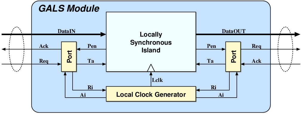
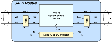 Figure 2.1:
An overview of a single GALS module with a input
and an output port.
The GALS module shown in Figure 2.1 is the basic building
block of a GALS system. At the heart of each GALS module is a locally
synchronous (LS) island. This block contains the functionality of
the module and is developed using conventional synchronous design
techniques. The clock signal for the LS island is generated by a local
clock generator. The data communication between GALS modules is governed
by specialized port controllers. These are asynchronous finite state
machines (AFSM) that can pause the local clock generator during data
transfers in order to ensure data integrity.
The GALS module uses a four-phase bundled data protocol to exchange
data with similarly designed GALS modules. Figure 2.2
shows a timing diagram with three consecutive clock cycles of a D-type
output port controller (which is later described in section 2.2.1).
The LS island uses the Port Enable (Pen) signal
to activate the port controller (A). The port controller immediately
sends a request signal (Ri) to pause the local clock
generator (B). The local clock generator issues the acknowledge signal
(Ai) only after it has stopped the propagation of
a new active clock edge (C). No new clock pulses will be generated
after this point, which effectively freezes the LS island. The port
controller then activates the Req signal (D), which
in turn tells the receiving GALS module that new data is available
for transfer. The port controller at the receiving GALS module goes
through similar stages and as soon as it is ready to accept new data,
it will acknowledge the request by activating the Ack
signal (E). At this moment, the local clocks of both GALS modules
are halted and the receiving GALS module can safely sample the data
. Afterwards, the handshake signals are returned to their initial
states and the local clocks are released. On the transmitting side
Req is deactivated first (F). Once the communication
partner deactivates Ack (G), the local clock generator
is released by deactivating Ri (H). The local clock
generator lowers Ai (J) and continues to generate
clock pulses (K). The port controller also sets the transfer acknowledge
(Ta) signal to notify the LS island of a successful
data transfer (L).
Figure 2.1:
An overview of a single GALS module with a input
and an output port.
The GALS module shown in Figure 2.1 is the basic building
block of a GALS system. At the heart of each GALS module is a locally
synchronous (LS) island. This block contains the functionality of
the module and is developed using conventional synchronous design
techniques. The clock signal for the LS island is generated by a local
clock generator. The data communication between GALS modules is governed
by specialized port controllers. These are asynchronous finite state
machines (AFSM) that can pause the local clock generator during data
transfers in order to ensure data integrity.
The GALS module uses a four-phase bundled data protocol to exchange
data with similarly designed GALS modules. Figure 2.2
shows a timing diagram with three consecutive clock cycles of a D-type
output port controller (which is later described in section 2.2.1).
The LS island uses the Port Enable (Pen) signal
to activate the port controller (A). The port controller immediately
sends a request signal (Ri) to pause the local clock
generator (B). The local clock generator issues the acknowledge signal
(Ai) only after it has stopped the propagation of
a new active clock edge (C). No new clock pulses will be generated
after this point, which effectively freezes the LS island. The port
controller then activates the Req signal (D), which
in turn tells the receiving GALS module that new data is available
for transfer. The port controller at the receiving GALS module goes
through similar stages and as soon as it is ready to accept new data,
it will acknowledge the request by activating the Ack
signal (E). At this moment, the local clocks of both GALS modules
are halted and the receiving GALS module can safely sample the data
. Afterwards, the handshake signals are returned to their initial
states and the local clocks are released. On the transmitting side
Req is deactivated first (F). Once the communication
partner deactivates Ack (G), the local clock generator
is released by deactivating Ri (H). The local clock
generator lowers Ai (J) and continues to generate
clock pulses (K). The port controller also sets the transfer acknowledge
(Ta) signal to notify the LS island of a successful
data transfer (L).
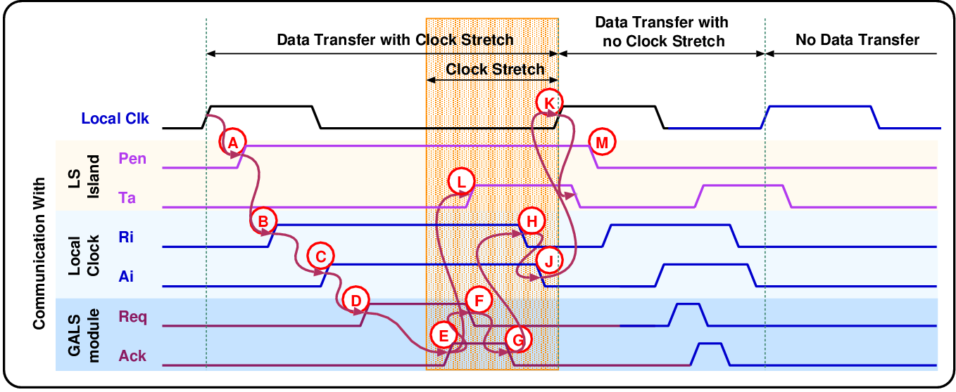
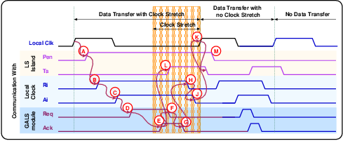 Figure 2.2:
Timing for a D-type output controller for
three consecutive clock cycles. In the first cycle shown, the environment
is slow to react to the Req signal. As a result
the clock is stretched until the data transfer has been processed.
The second cycle shows another transfer where the handshake finishes
within the clock cycle. Finally in the third cycle, the Pen
signal is not enabled, and no data transfer is initiated.
In the communication scheme presented above, the LS island starts
the data transfer by activating the Pen signal.
To enable data transfers in consecutive clock cycles, Muttersbach
used a two phase protocol only for the Pen signal.
A new data transfer is initiated by changing the value of Pen.
This can be seen in figure 2.2, in the first cycle
the data transfer is initiated by a rising transition of the Pen
signal (A) and in the second cycle a new data transfer is initiated
by a falling transition of Pen (M). In the third
cycle, Pen stays low, and no data is transferred.
When compared to a four-phase realization, this arrangement doubles
the throughput of the data connection at the expense of more complex
port controllers.
In the first clock cycle shown in figure 2.2, the
local clock is stretched as the sending module awaits the Ack
signal, effectively slowing the sending module. If both GALS modules
are ready to communicate, the data transfer can be completed without
stretching the local clock at all as illustrated in the second clock
cycle in figure 2.2.
Figure 2.2:
Timing for a D-type output controller for
three consecutive clock cycles. In the first cycle shown, the environment
is slow to react to the Req signal. As a result
the clock is stretched until the data transfer has been processed.
The second cycle shows another transfer where the handshake finishes
within the clock cycle. Finally in the third cycle, the Pen
signal is not enabled, and no data transfer is initiated.
In the communication scheme presented above, the LS island starts
the data transfer by activating the Pen signal.
To enable data transfers in consecutive clock cycles, Muttersbach
used a two phase protocol only for the Pen signal.
A new data transfer is initiated by changing the value of Pen.
This can be seen in figure 2.2, in the first cycle
the data transfer is initiated by a rising transition of the Pen
signal (A) and in the second cycle a new data transfer is initiated
by a falling transition of Pen (M). In the third
cycle, Pen stays low, and no data is transferred.
When compared to a four-phase realization, this arrangement doubles
the throughput of the data connection at the expense of more complex
port controllers.
In the first clock cycle shown in figure 2.2, the
local clock is stretched as the sending module awaits the Ack
signal, effectively slowing the sending module. If both GALS modules
are ready to communicate, the data transfer can be completed without
stretching the local clock at all as illustrated in the second clock
cycle in figure 2.2.
2.2.1
Port Controller Types
The timing diagram in figure 2.2 shows an output
port controller that suspends the local clock of the LS island as
soon as it is ready to transmit data. This is a desired behavior for
a system that can not continue without completing the present data
transfer. Muttersbach named the input and output ports that halt the
clock immediately 'Demand Type' (D-type) ports.
In some cases however, a GALS module may initiate a data transfer
and continue operating up to a point where a data dependency occurs.
The 'Poll Type' (P-type) ports were developed to serve this purpose.
In contrast to a D-type output port, a P-type output port first activates
the Req signal to tell its communication partner
that it is ready to send data. Until an Ack signal
is received the local clock is not paused and the LS island continues
to operate normally. As soon as the P-type controller receives an
Ack it issues a Ri signal to pause
the local clock generator momentarily. Then, after the four-phase
handshake is completed and all control signals return to their initial
levels. For P-type controllers the Ta signal is
very important as the LS island needs to constantly observe the value
of Ta to determine the status of the last data transfer.
The first GALS demonstrator circuit presented in [MVF00]
was designed by using only point-to-point connections with only the
two port controller types mentioned above. A large set of additional
port controllers was developed by T. Villiger to support multi-point
interconnections [Vil05].
There are various methods that can be applied to describe ASFMs that
make up the port controllers. Muttersbach used the 'Enhanced Burst
Mode' [YD99a,YD99b] specification to describe the port controllers.
The 3D software developed by K. Yun converts the port specification
into Boolean equations which are then mapped to standard cells manually.
2.2.2
Local Clock Generator
The GALS methodology developed by Muttersbach relies on a pausable
local clock generator to prevent metastability during data transfers.
Therefore, a fast and reliable local clock generator is the key to
a successful GALS implementation. The block diagram of the local clock
generator is shown in figure 2.3. The
clock generator is basically a ring oscillator whose period can be
controlled by programming the delay line. The arbitration block provides
the pausability feature to the clock generator.
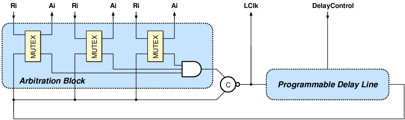
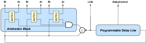 Figure 2.3:
Simplified block diagram of a
pausable local clock generator.
The local clock generator provides several ports, each of which, when
activated, can pause the clock. For each port, the pause request signal
(Ri) is combined with the output of the delay line,
using a mutual exclusion element (MutEx). MutEx is a specialized circuit
that allows only one of its outputs to be at logic-1 at a certain
time. There are different implementations of the MutEx. A twelve transistor
full-custom implementation that is used for the GALS implementations
in the UMC 0.25 m process can be seen in figure 2.4.
A rising edge of the local clock can only propagate through the arbitration
block if the Ri signals of all ports are logic-0.
The output of the arbitration block is combined using a Muller-C gate
that essentially only changes its output when both of its inputs are
in agreement.
Figure 2.3:
Simplified block diagram of a
pausable local clock generator.
The local clock generator provides several ports, each of which, when
activated, can pause the clock. For each port, the pause request signal
(Ri) is combined with the output of the delay line,
using a mutual exclusion element (MutEx). MutEx is a specialized circuit
that allows only one of its outputs to be at logic-1 at a certain
time. There are different implementations of the MutEx. A twelve transistor
full-custom implementation that is used for the GALS implementations
in the UMC 0.25 m process can be seen in figure 2.4.
A rising edge of the local clock can only propagate through the arbitration
block if the Ri signals of all ports are logic-0.
The output of the arbitration block is combined using a Muller-C gate
that essentially only changes its output when both of its inputs are
in agreement.
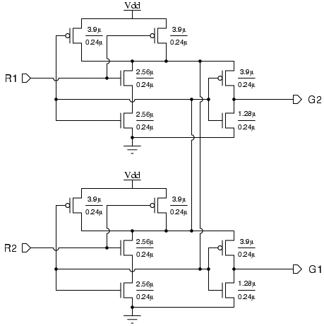
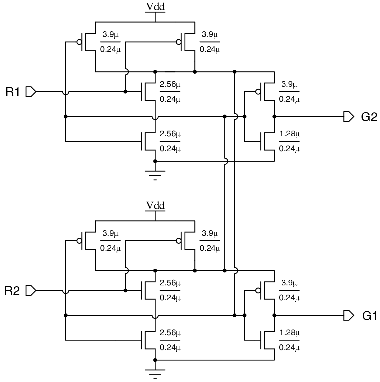
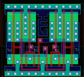 Figure 2.4:
The Mutual Exclusion element, transistor
schematic (left) and layout (right) for the UMC 0.25 m
technology.
As long as one (or more) of the Ri signals is at
logic-1, a new clock pulse will not be generated and the local clock
will effectively be paused. The next rising edge will propagate through
the Muller-C gate only after the blocking Ri signal
is returned to logic-0. The MutEx directly generates the clock pause
acknowledge signal (Ai) as well. If the Ri
request is able to propagate to the Ai output, the
clock is effectively paused3. Ai will only return to logic-0 after Ri
is lowered.
The number of ports of a pausable local clock generator is not really
limited, however combining the outputs of multiple ports reduces the
maximum attainable clock frequency somehow. Local clock generators
with up to 8 ports have been successfully implemented in practice.
The frequency of the local clock generator can be adjusted using the
programmable delay line. However, during normal operation the clock
frequency is not changed. The delay line is usually programmed during
startup to match the critical path of the module it is connected to.
Having a programmable delay line allows the same clock generator to
be used for GALS modules with different clock frequencies. Especially
for aggressive designs, the exact value of the maximum allowable clock
period is not known until the very end of design process. A programmable
delay line is practical for such designs as well, since the clock
period does not need to be fixed as long as it is within the range
of the local clock generator.
Figure 2.4:
The Mutual Exclusion element, transistor
schematic (left) and layout (right) for the UMC 0.25 m
technology.
As long as one (or more) of the Ri signals is at
logic-1, a new clock pulse will not be generated and the local clock
will effectively be paused. The next rising edge will propagate through
the Muller-C gate only after the blocking Ri signal
is returned to logic-0. The MutEx directly generates the clock pause
acknowledge signal (Ai) as well. If the Ri
request is able to propagate to the Ai output, the
clock is effectively paused3. Ai will only return to logic-0 after Ri
is lowered.
The number of ports of a pausable local clock generator is not really
limited, however combining the outputs of multiple ports reduces the
maximum attainable clock frequency somehow. Local clock generators
with up to 8 ports have been successfully implemented in practice.
The frequency of the local clock generator can be adjusted using the
programmable delay line. However, during normal operation the clock
frequency is not changed. The delay line is usually programmed during
startup to match the critical path of the module it is connected to.
Having a programmable delay line allows the same clock generator to
be used for GALS modules with different clock frequencies. Especially
for aggressive designs, the exact value of the maximum allowable clock
period is not known until the very end of design process. A programmable
delay line is practical for such designs as well, since the clock
period does not need to be fixed as long as it is within the range
of the local clock generator.
2.2.3 Timing Constraints
Depending on the methodology used, several timing assumptions are
made during the design phase. As an example, for synchronous designs
it is assumed that all inputs of flip-flops are stable before the
clock pulse arrives (setup-time constraint) and that they remain stable
until the flip-flop has safely sampled its input (hold-time constraint).
The circuit will only function correctly if these timing assumptions
hold true.
In circuits that use multiple clock domains, this can be tricky, especially
on the boundaries between the clock domains. Furthermore, with decreasing
feature sizes, an ever increasing portion of the timing is determined
by the interconnections. These can only be accurately determined at
the final stages of the design, where placement and routing is completed.
The goal of GALS is to handle most of the timing problems that arise
in systems with multiple clocking domains, and to impose the least
amount of restrictions on the designer of LS islands. To achieve this
goal, components of the GALS system must satisfy several timing requirements.
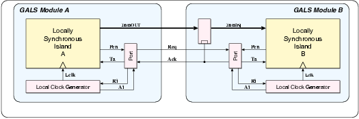 Figure 2.5:
Two interconnected GALS modules. The
latch at the data inputs in GALS module B is required to make sure
that the data is still present when the first data edge appears after
the data transfer.
The port controllers used in GALS are obtained using asynchronous
synthesis tools [CKK+97,YD99a], that convert state transition
diagrams into boolean equations. Depending on the specific asynchronous
description used, several timing constraints have to be met to ensure
proper operation. Similar constraints may exist for the communication
between port controllers as well.
The data inputs and outputs are also of concern. Muttersbach strongly
advises to use registers at the input and outputs of the LS islands.
For synchronous systems, this represents the best case in terms of
input and output timing. However, this is not sufficient. Figure 2.5
shows two interconnected GALS modules where the data input of GALS
module B is latched by a handshake signal. The latch is only active
during the handshake and it stores the data outputs of GALS
module A during the data transfer. This is necessary because after
the data transfer, LS island A may receive an active clock
edge before LS island B. This could change the output of LS
island A before LS island B has a chance to sample its inputs 4.
The two control signals Pen and Ta
have additional problems. Since Pen is used to activate
an AFSM, it must be free of glitches. The easiest method to guarantee
this is to use a register for the Pen signal. The
Ta signal is used to determine if a pending data
transfer has been completed. This signal is required for P-type controllers,
where the local clock is only halted during the data transfer. The
Ta signal is generated by the port controller and
sampled by the LS island. This signal must satisfy several timing
constraints to function properly.
Figure 2.5:
Two interconnected GALS modules. The
latch at the data inputs in GALS module B is required to make sure
that the data is still present when the first data edge appears after
the data transfer.
The port controllers used in GALS are obtained using asynchronous
synthesis tools [CKK+97,YD99a], that convert state transition
diagrams into boolean equations. Depending on the specific asynchronous
description used, several timing constraints have to be met to ensure
proper operation. Similar constraints may exist for the communication
between port controllers as well.
The data inputs and outputs are also of concern. Muttersbach strongly
advises to use registers at the input and outputs of the LS islands.
For synchronous systems, this represents the best case in terms of
input and output timing. However, this is not sufficient. Figure 2.5
shows two interconnected GALS modules where the data input of GALS
module B is latched by a handshake signal. The latch is only active
during the handshake and it stores the data outputs of GALS
module A during the data transfer. This is necessary because after
the data transfer, LS island A may receive an active clock
edge before LS island B. This could change the output of LS
island A before LS island B has a chance to sample its inputs 4.
The two control signals Pen and Ta
have additional problems. Since Pen is used to activate
an AFSM, it must be free of glitches. The easiest method to guarantee
this is to use a register for the Pen signal. The
Ta signal is used to determine if a pending data
transfer has been completed. This signal is required for P-type controllers,
where the local clock is only halted during the data transfer. The
Ta signal is generated by the port controller and
sampled by the LS island. This signal must satisfy several timing
constraints to function properly.
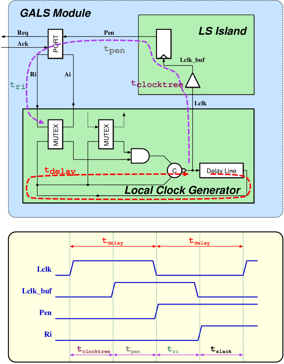
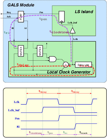 Figure 2.6:
Timing constraints of a D-type
port. Once activated the port controller must be able to halt the
local clock generator before a new clock edge is generated. If the
clock tree insertion delay tclocktree is sufficiently large,
this timing constraint can not be satisfied.
Specialized port controllers may have additional timing constraints.
As an example, Muttersbach presents D-type port controllers that are
capable of exchanging data during consecutive clock cycles. As soon
as a D-type port is enabled by the Pen signal, it
immediately activates Ri to stop the local clock
generator. This is shown in figure 2.6.
Practically all LS islands need a clock tree to distribute the clock
signal. Depending on the size of the LS island, this requires the
insertion of several levels of buffers in the clock signal path, resulting
in a clock tree insertion delay tclocktree. The clock signal
that arrives at the flip-flop generating the Pen
signal will be delayed by tclocktree. The flip-flop generating
the Pen signal will have a finite propagation delay of tpen
and, finally, the Ri signal will be produced with
a delay of tri. The sum of all three delays must be less than
the nominal period of the local clock generator if the port controller
is expected to send data every clock cycle. Aggressive designs may
require significant amounts of tclocktree to function properly.
The clock tree insertion delay may even exceed the clock period. Other
solutions need to be explored for such systems.
Figure 2.6:
Timing constraints of a D-type
port. Once activated the port controller must be able to halt the
local clock generator before a new clock edge is generated. If the
clock tree insertion delay tclocktree is sufficiently large,
this timing constraint can not be satisfied.
Specialized port controllers may have additional timing constraints.
As an example, Muttersbach presents D-type port controllers that are
capable of exchanging data during consecutive clock cycles. As soon
as a D-type port is enabled by the Pen signal, it
immediately activates Ri to stop the local clock
generator. This is shown in figure 2.6.
Practically all LS islands need a clock tree to distribute the clock
signal. Depending on the size of the LS island, this requires the
insertion of several levels of buffers in the clock signal path, resulting
in a clock tree insertion delay tclocktree. The clock signal
that arrives at the flip-flop generating the Pen
signal will be delayed by tclocktree. The flip-flop generating
the Pen signal will have a finite propagation delay of tpen
and, finally, the Ri signal will be produced with
a delay of tri. The sum of all three delays must be less than
the nominal period of the local clock generator if the port controller
is expected to send data every clock cycle. Aggressive designs may
require significant amounts of tclocktree to function properly.
The clock tree insertion delay may even exceed the clock period. Other
solutions need to be explored for such systems.
2.3 GALS-Based Solutions
The GALS design methodology allows designers to partition a large
system into several sub-modules, each of which can be optimized independently.
Since the modules do not rely on a global clock to communicate with
each other, less effort is required to maintain data integrity on
data transfers between modules. Designers using GALS have more freedom
to improve the performance of the system. However, this does not imply
that simply using GALS will automatically result in a system that
is faster, smaller, consumes less power, and is designed in a shorter
time.
Most of the GALS systems presented in the literature are based on
a working synchronous design. This design is then partitioned into
several independent GALS modules in a process that is known as GALSification.
Such GALSified systems are at heart still synchronous designs. Several
decisions during the design phase of such circuits are based on synchronous
constraints. Such systems are less likely to harvest all advantages
being offered by GALS, than systems that were from the onset designed
with GALS in mind.
The following is a brief discussion of what can be expected by using
the GALS methodology for various design parameters:
The technological advances in micro-electronic fabrication have enabled
the performance of integrated circuits to increase at a rate defined
by Moore's Law for the last 4 decades. The factors that resulted in
increased performance (smaller transistors, denser circuits, faster
switching times) have also increased the amount of power dissipated
per unit area. Contemporary high-end micro-processors reach power
densities in excess of 100 W/cm2, which is an order of magnitude
more than a heating plate used in the kitchen. Therefore reducing
the power consumption of digital circuits is of paramount importance.
In a GALS system, modules that are not used frequently can be made
to consume less power by either pausing their local clocks until they
are needed, or by simply using a reduced local clock frequency (and/or
supply voltage) for that particular module. It is also possible to
optimize this approach by designing systems that dynamically adjust
their frequency and or supply voltage on demand.
Pausing the local clock of a GALS module during times of inactivity
is basically equivalent to clock gating at the module level. It can
be easily realized by using D-type ports. During a data transfer between
GALS modules the local clock will be paused until the interconnected
GALS module is ready to send/receive data. While the module is in
this 'wait' state, no new clock pulse will be generated, and the module
will not consume dynamic power. The power saving that can be achieved
by this method depends entirely on how often the module is utilized.
Similar gains can also be obtained by using clock gating within the
module as well.
The dynamic power consumption Pdyn of a CMOS circuit is known
to be proportional to the activity factor a, the amount of
switched capacitance C, the clock frequency f, and to the square
of the supply voltage Vdd as given by the well known relation
2.1:
It follows from this relation that, if a module is used less frequently,
it is more power efficient to use a lower Vdd which in turn
reduces the maximum operating frequency f. So rather than having
a fast module (with nominal Vdd) that runs for a short time
and then pauses, it is better to use a slow module (with reduced Vdd)
that runs at a speed where it does not pause at all. The aim of Dynamic
Voltage and Frequency Scaling (DVFS) systems is to achieve this compromise
automatically. GALS systems seem to be well suited for implementing
DVFS systems since the activity of a module can easily be determined
by monitoring the local clock, or the handshake signals. Based on
results obtained through simulations, this idea looks promising. In
a GALS system specialized for real-time applications, Bhunia et al.
[BDBR05] claim up to 67% improvement in throughput per watt
over a synchronous implementation.
While the idea seems interesting, there are some problems associated
with this approach. Modern devices require very low voltages for power
supply around (or even below) 1 V. This does not leave much noise
margin for correct operation, and the supply voltage can not be reduced
much further to reduce power consumption. Also communication between
modules that use different input/output voltages will require level
converter circuits.
Early implementations of GALS were based on a premise that using this
methodology would result in lower power consumption. While several
aspects of the GALS design methodology are in line with practices
developed to reduce power consumption, just using GALS does not result
in achieving low power designs.
2.3.2 High Performance
The operating frequency of a synchronous system has to accommodate
the worst-case propagation delay in the circuit. A self-timed implementation
of the same circuit would have a similar performance under the same
worst-case condition. However, an optimal self-timed system would
be able to finish processing other non-worst-case conditions faster,
and consequently, over a large range of samples, it would have an
average-case performance that exceeds that of the synchronous system5. For systems where such an average-case performance deviates significantly
from worst-case performance (like a ripple-carry adder for instance),
self-timed systems can achieve a higher throughput than their synchronous
counter-parts. A GALS system may benefit in a similar way as demonstrated
by the following hypothetical example:
Assume a system that performs a single operationA, followed
by ten operationB. In a synchronous system the slower of both
operations would determine the overall clock rate. Let us assume that
the critical path of operationA is 3 ns and that of operationB
is 2 ns. The synchronous system would require eleven clock cycles
of 3 ns totaling 33 ns.
A GALS system that implements each operation as a separate GALS modules
would compute operationA within 3 ns and then wait for
the result of ten operationB that could be calculated within
20 ns. Communicating between GALS islands adds latency to the
system. Even if 3 ns communication overhead is added to the system,
the GALS system would be able to complete both operations in 26 ns,
more than 20% faster than the synchronous system.
The example given above is overly simplistic and makes several assumptions
for a GALS favorable outcome. Nonetheless it demonstrates that under
certain conditions GALS systems can indeed increase the throughput,
or at least can compensate for the additional latency incurred by
communication between GALS modules. A more detailed analysis for a
high performance micro-processor architecture is given in [SAM+04].
2.3.3 Ease of Integration
The GALS design methodology allows a very large system to be partitioned
into smaller modules, each of which can be optimized independently.
At the top level, the designer only has to realize the interconnections
between GALS modules which have minor or no timing constraints set
on them6. This is in stark contrast to synchronous system-on-chip solutions,
where most of the design effort is concentrated to ensure proper distribution
of the clock signal and timely arrival of data connections between
functional blocks.
In a GALS system, the communication and the functionality are clearly
separated. The communication between GALS modules is handled by the
asynchronous port controllers, and the functionality is provided by
the LS island. The designer of the LS island can therefore focus entirely
on the functionality, without worrying about the data communication
to other LS islands. In synchronous systems, the sub-blocks typically
use the system clock, or derive their own clocks from a central clock,
so that inter-block timing constraints can be met. This frequently
results in over-constrained sub-blocks, that have to be designed with
tighter timing constraints than is really necessary. Moreover, such
a sub-block can not always be re-used in a different system, as the
timing requirements for this new system may differ from that of the
original system. In a GALS system, this is not necessary, the LS island
designers are completely free to choose an appropriate local clock
rate that fulfills the requirements of the system. The GALS module
can be readily re-used since its timing is independent from the environment.
While the goal of earlier GALS implementations centered on improved
performance metrics, such as lower power consumption and increased
throughput, later publications highlighted the ease of integration
as its main advantage.
2.3.4 Secure Applications
In the fourth Workshop on Asynchronous Circuit Design held in June
2004 in Turku, Finland, a special session was held for a joint Strengths
Weaknesses Opportunities and Threats (SWOT) analysis for asynchronous
circuits. The question that defined the opportunities was:
"Assume you were asking a billion dollars from an investor (to
develop self-timed circuits), what would be your strongest argument
?"
Interestingly, cryptographic systems and smart cards was the most
commonly stated answer. Practical realizations of cryptographic algorithms
in hardware suffer from so-called side channel attacks that can be
exploited to compromise the security of the system. Over the years,
various publications [SMBY05,
TV03,
FML+04,
YFP03]
have claimed that asynchronous circuits are less susceptible to such
attacks, mainly since they do not rely on a synchronous clock (a more
detailed discussion of this topic can be found in section 3.5.1).
While GALS circuits employ asynchronous communication at the top level,
the main functionality is provided by LS islands which are synchronous.
Therefore, it may be argued that GALS systems are as susceptible to
side channel attacks as their synchronous counterparts. The design
presented in chapter 4 is the first application
of GALS in a cryptographic system and uses several features of GALS
design to improve side channel security.
Cryptographic hardware implementations are in widespread use for more
than 30 years. Despite all the effort of the cryptographic community,
the threat of side channel attacks against hardware implementations
was first discovered in 1996. Evaluating the security of a countermeasure
is not trivial. While a novel circuit design method may prove to be
effective against a particular side channel attack, it may be vulnerable
to other (similar) attacks. It could be argued that, asynchronous
circuits, which are not used as widely, have not been scrutinized
at the same level as synchronous circuits, which has helped to bolster
their reputation of being more 'secure'. The only way to evaluate
the security of new ideas, including the GALS-based design presented
in this thesis, is to make them available to the cryptographic community
for pro-longed analysis.
File translated from
TEX
by
TTH,
version 3.77.
On 20 Dec 2006, 15:44.