GALS System Design:
Side Channel Attack Secure Cryptographic Accelerators
Chapter 5:
Designing GALS Systems
Disclaimer:
This is the www enabled version of my thesis. This has been converted from
the sources of the original file by using TTH, some perl
and some hand editing.
There is also a PDF.
This is essentially as it is, but includes formatting for A4, and some of the color pictures
from the presentation.
Contents
1 Introduction
2 GALS System Design
3 Cryptographic Accelerators
4 Secure AES Implementation Using GALS
5 Designing GALS Systems
5.1 Design Automation Issues
5.2 Designing Asynchronous Finite State
Machines
5.2.1 Port Controllers in Acacia
5.2.2 Data Exchange between David and Goliath
5.2.3 Data Exchange between Goliath and Synchronous Interface
5.3 Testing Acacia
5.4 Adapting Modules for GALS
5.5 Related Research Directions
5.5.1 Network-on-Chip Systems
5.5.2 Dynamic Voltage and Frequency Scaling
5.5.3 Latency-Insensitive Design
6 Conclusion
A 'Guessing' Effort for Keys
B List of Abbreviations
B Bibliography
B Footnotes
Chapter 5
Designing GALS Systems
The main advantage of the GALS design methodology over other self-timed
design methods is that only a well-defined, small fraction of a GALS
system contains self-timed circuits. This has two important consequences:
- The majority of a GALS system can be designed using synchronous design
methods.
- The problems commonly related to self-timed design are limited in
complexity and can be practically solved with non-optimal methods.
As a result, the design of a GALS system does not differ significantly
from a standard synchronous design. There are obviously several GALS
specific issues that have to be addressed while designing GALS systems.
This chapter discusses these issues, and basically describes the differences
between standard synchronous design flow and GALS design flow.
5.1
Design Automation Issues
Over the years many EDA companies have developed powerful tools to
support a well established synchronous design flow. Self-timed design
methodologies on the other hand, are not used as widely, especially
for industrial designs. The EDA industry has therefore not invested
in tools that support self-timed design flows40. As a result, small research groups have been left to develop tools
for self-timed design. These efforts have been further hampered by
the fact that there is no unified design methodology. Every research
group has developed its own approach to design self-timed circuits.
As with every newly proposed design methodology, the industrial acceptance
of the GALS design methodology depends mainly on how well suited it
is to design automation. Fortunately, up to 99% of a GALS system
consists of standard synchronous design, and for the most part a standard
design flow can be used. A design automation solution has to solve
the following issues:
- Develop a library with self-timed port controllers
The port controllers are the only real self-timed elements in the
GALS system. They are realized as asynchronous finite state machines
(AFSMs) and, depending on the approach used, can be synthesized using
a variety of tools like Petrify [CKK+97],
3D [YD99a]
or Minimalist [FNT+99]. The end result is a gate level netlist
that typically consists of 5 to 20 standard cells of the target process.
If the port controllers can be standardized ,it would also be possible
to use transistor level optimized port controllers that are realized
as standard cells.
These port controllers are (usually) not design specific. They can
be designed, optimized and verified separately. In addition, generally
only a very limited set of port controllers is used. As an example,
Acacia uses only three different port controllers. A detailed
description of how the ports were developed for Acacia can
be found in section 5.2.
- Develop the local clock generator
The local clock generator is a critical element of the GALS system.
The clock generator relies on a special MutEx element that needs to
be provided as part of the standard cell library (see section 2.2.2
for details). The clock period is determined by using a delay line.
Depending on the resolution required, a number of different methods
can be used to realize the delay line[OVG+02]. Similar
to the self-timed port controllers, the local clock generator is not
design specific and can be designed and optimized separately.
- Providing a partitioning method
Functionality, separate clock domains, and the gate count can all
be used as parameters that determine the partitioning. Ideally, a
GALS partition needs to be able to work on its own for longer periods
of time and should consist of a single clock domain. In addition,
the LS island should be of reasonable size. It should be sufficiently
large to justify the overhead, but should not be overly large 41.
This is probably the only part of the GALS design methodology that
is not yet supported by design automation tools. It requires manual
skill and experience to determine a partition that will result in
an efficient GALS system.
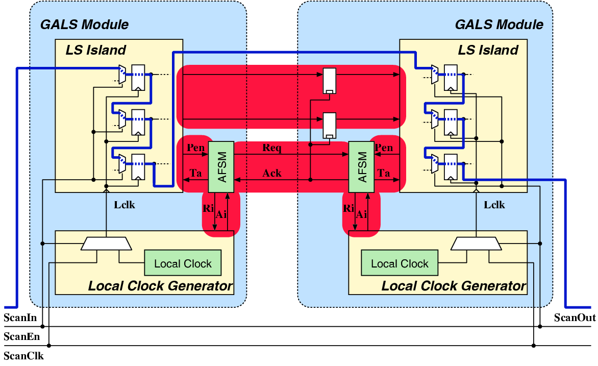
- Assembling individual GALS modules
A GALS module is created by encapsulating the LS island by a self
timed wrapper that contains the local clock generator and the asynchronous
port controllers. By itself, this is not a very difficult task and
can be easily automated. Some elements of the self-timed wrapper require
special attention from certain design tools. For example, the structure
of the port controllers may not be optimized by the synthesis tool.
Similarly, the standard cells making up the delay line elements within
the local clock generator should not be placed randomly. These are,
comparatively, minor issues and can easily be added to standard design
scripts.
- Verifying the timing constraints of the asynchronous connections
The asynchronous port controllers need to meet certain timing constraints
to guarantee proper operation. For most circuits, it is only possible
to determine the final timing after the placement and routing of the
system has been completed. The timing of all ports controllers must
be verified at this stage. Standard timing analyzers usually require
a synchronous clock to perform the timing analysis, and can not automatically
be used to verify self-timed port controllers.
However, almost all industrial timing analyzers can be programmed
to measure worst case and best case propagation delays through any
given path. Since the asynchronous port controllers contain few standard
cells, all relevant path delays can be calculated with reasonable
effort. These results can then be processed to determine whether or
not any timing assumptions have been violated [GOV+03b].
Interestingly, most of the timing violations occur through fast connections.
Resolving such conflicts, even at later stages of a design is very
easy. Additional buffers are placed in the signal path. It is also
possible to design the port controllers more conservatively from the
beginning. In this way, the timing verification effort can be reduced
significantly as well.
- Assembling the GALS system
The GALS system basically consists of interconnected GALS modules.
In a synchronous design methodology, the back-end design is a difficult
task that requires considerable effort which increases with increasing
circuit size.
In contrast, the top-level design for a GALS system is very straightforward.
The modules are simply placed and the interconnections are made. The
GALS design methodology is especially suited to a hierarchical design
methodology, where parts of the design are placed and routed independently.
The design flow used for Shir-Khan, a fairly large GALS system
consisting of 25 different GALS modules, can be seen in figure 5.1.
There are five different design levels at Shir-Khan:
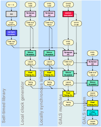 Figure 5.1:
Design flow used for the Shir-Khan
system.
Figure 5.1:
Design flow used for the Shir-Khan
system.
- The Self-Timed Library
Shir-Khan was designed to investigate different multi-point
interconnect architectures for GALS [Vil05]. This required
a large collection of experimental port controllers. Contrary to a
more traditional GALS design, the self-timed library used in Shir-Khan
contains 57 different port controllers. All of the ports were synthesized
by the 3D tool. The generated boolean equations were mapped to standard
cells of the target technology by the help of a custom tool called
eqn2gate 42.
- The Local Clock Generator
An important requirement of the local clock generator was a high period
resolution. This required the design of an additional standard cell
to be able to control the delay line with sub-gate delay accuracy.
To achieve optimum performance, the local clock generator was designed
as a hierarchical module. The design was synthesized, placed and routed
separately and instantiated as a macro cell by the GALS modules.
- The SIMD Micro-Controller
The LS island of all GALS modules consisted of a specialized 4-bit
micro-controller named port processor. The port processor
was designed specifically to activate any combination of 4 input and
output ports simultaneously. It was used to generate different traffic
patterns on the multi-point interconnects. The port processor
was designed using a standard synchronous design flow.
- GALS Modules
Shir-Khan has 25 GALS modules and a total of 181 port controller instantiations.
A special design automation script called moduleassembler was
written to automate the design process. moduleassembler used
a textual description of the GALS system, and automatically generated
the VHDL code for each GALS module. Furthermore, it generated tool-specific
scripts to complete the design flow. All GALS modules in Shir-Khan
were assembled automatically by scripts and source code generated
by moduleassembler. Similar to the local clock generator each
GALS module was designed as a hierarchical module.
- GALS System
The remaining tasks of the design was to instantiate, place and route
the GALS modules at the top-level43. The source code of the top-level instance was made manually. The
GALS modules were placed on the chip and a power routing was devised.
The signal interconnections were made using standard routing tools.
The scripts developed for Shir-Khan could have been modified
to support the design flow for Acacia as well. However, since
Acacia is much smaller in comparison and uses only two unique
GALS modules with only three port instantiations, it was more practical
to conduct the design flow manually.
The main difference between the two designs is in the back-end design
flow. In Shir-Khan, Silicon Ensemble from Cadence Design Systems
was used. However, this older tool does not directly support a hierarchical
design flow. Rather complex design scripts which were automatically
generated by moduleassembler had to be used to emulate a hierarchical
design flow. Acacia used SOC-Encounter from Cadence Design
Systems that inherently supports a hierarchical design flow. This
design flow is well suited for GALS and made it considerably easier
to design the chip.
5.2
Designing Asynchronous
Finite State
Machines
The basic design principle between synchronous and asynchronous finite
state machines (AFSMs) are very similar. Both types of state machines
preserve their state until certain conditions are met. The input signals
and the present state of the machine is used to determine the next
state. In a synchronous finite state machine, the next state change
occurs after the next active clock event, whereas an AFSM moves to
the next state as soon as the conditions to change the state are met.
This results in extremely fast state transitions. Since decisions
are sudden, all input signals that are used for these decisions have
to be stable. AFSMs are very sensitive to glitches at their inputs44. The synthesis of AFSMs is therefore more involved than their synchronous
counterparts.
There are different classes of self-timed circuits [SF01].
Each class has its own set of assumptions that results in slightly
different realizations. The most robust and general class of self-timed
circuits are delay-insensitive (DI) circuits. These circuits will
function correctly regardless of the gate and wire delays in the circuit.
Unfortunately, only few practical DI circuits can be realized. A more
practical class of self-timed circuits is obtained from DI circuits
by assuming that two wires that split from a common wire have the
same unbounded delay. The class of self-timed circuits that function
correctly under this isochronic-fork assumption are known as Quasi-delay-insensitive
(QDI) circuits. Even less assumptions are made for Speed-independent
(SI) circuits that only assume bounded gate delays but no wire delays.
At first sight this assumption seems unrealistic for modern integrated
circuits. However, circuits whose wire delays are lumped into gate
delays can still be considered speed-independent.
Before an AFSM can be synthesized, it needs to be described in a way
that is convenient for the developer and understandable for the tools.
A popular method for expressing AFSMs is using signal transition graphs
(STG), that is essentially a simplified form of the Petri-Nets. An
example STG can be seen in figure 5.4. In this graph,
the boxes represent a signal transition. The signal name followed
by a '+' represents a raising transition of the signal, and similarly
a '-' represents a falling transition. Solid and dotted lines are
used to represent outputs and inputs respectively. The large dot is
called a "token" and represents the current state of the system.
The STG can also be represented in machine readable form. The following
is a textual description of the STG seen in in figure 5.4.
-
.model d2g
.inputs Pen Ack Ai
.outputs Req Ri Ta
.graph
Pen+ Req+
Req+ Ack+
Ack+ Ri+
Ri+ Ai+
Ai+ Req- Ta+
Ta+ Pen-
Req- Ack-
Ack- Ri-
Ri- Ai-
Ai- Pen-
Pen- Ta-
Ta- Pen+
.marking{<Ta-,Pen+>}
.end
-
An AFSM synthesis tool is able to convert this description into a
set of boolean equations, or even a gate-level netlist. Depending
on the self-timed circuit style, the AFSMs are synthesized using certain
timing assumptions. In the final circuit implementation, these assumptions
must still hold true. For modern IC technologies the interconnection
delays can vary significantly depending on the placement and routing
of the final circuit. It is important to verify the correctness of
the AFSMs after final placement and routing.
5.2.1 Port Controllers in Acacia
Although a library of port controllers developed for earlier GALS
projects was available at the start of the project, a new set of port
controllers were specifically developed for Acacia. The main
reasons for the additional effort are the following:
- Level sensitive port enable
In an effort to enable data transfers at every clock cycle, the port
controllers developed by Muttersbach used an edge sensitive port enable
signal. This practically doubles the number of states in the AFSM
and results in slightly larger realizations. The GALS modules in Acacia
were explicitly designed not to transfer data during consecutive clock
cycles. Therefore, this overhead was deemed to be unnecessary.
- Different transfer acknowledge
The transfer acknowledge signal (Ta) as implemented
by Muttersbach uses a flip-flop that could be set during data transfer
and would be cleared by the first active clock edge. The most important
problem with this approach is that the Ta signal
must be sampled immediately since the first clock cycle will clear
the information. In addition, the clock signal used in the port controller
must be balanced with respect to that used in the LS island. Acacia
uses a more "relaxed" Ta signal that remains
active until a new data transfer starts.
- One-sided port
The interface between Goliath and the synchronous environment
is special since only the local clock of Goliath can be paused
for synchronization. A special port that is able to transfer data
safely between the synchronous environment and a GALS module was designed
for this purpose. The port is called one-sided since it can only influence
one side of the data transfer.
Mainly due to the level sensitive input to enable the port controllers,
earlier GALS ports designed by Muttersbach used the "extended
burst mode" circuit description [YD99a] and were synthesized
using the 3D tool. The port controllers in Acacia are speed-independent
AFSMs that are synthesized from signal transition graphs using a tool
called Petrify [CKK+97].
The idea to use three independently clocked GALS modules is a key
part of the DPA countermeasures implemented in Acacia. The
pausable clock generator is used to ensure data integrity during data
transfers between GALS modules. If the clock is paused for longer
durations, an attacker could potentially determine the time when two
modules exchange data, and could use this information to refine the
attack. To deny the attacker any such opportunity, the port controllers
in Acacia were designed to reduce the synchronization time
as much as possible. These ports work similar to P-type ports developed
by Muttersbach. The port controller pauses the local clock only momentarily
when its communication partner has signaled that it is ready for data
transfer.
5.2.2 Data Exchange between David and Goliath
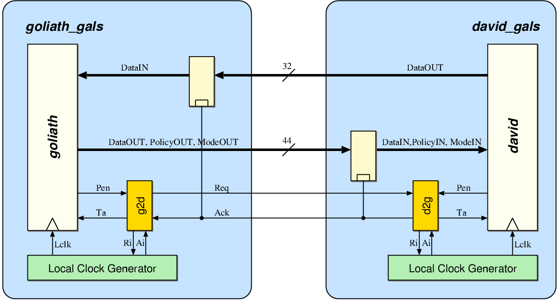
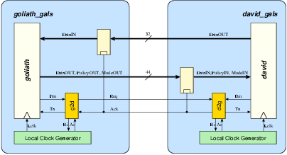 Figure 5.2:
The interface between
David and Goliath.
The block diagram in figure 5.2
shows the data communication channel between David and Goliath.
There are two separate port controllers, d2g on the David
side and g2d on the Goliath side. Unlike earlier GALS
implementations, the port controllers in Acacia are bi-directional.
Once both GALS modules are synchronized, both modules exchange data.
Figure 5.2:
The interface between
David and Goliath.
The block diagram in figure 5.2
shows the data communication channel between David and Goliath.
There are two separate port controllers, d2g on the David
side and g2d on the Goliath side. Unlike earlier GALS
implementations, the port controllers in Acacia are bi-directional.
Once both GALS modules are synchronized, both modules exchange data.
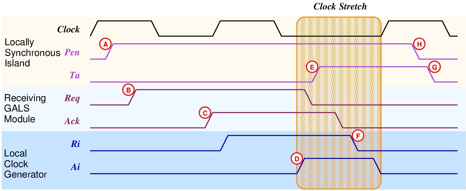
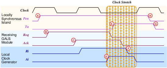 Figure 5.3:
Timing diagram for the d2g
port. Notice that this timing is substantially different from the
GALS port timing shown in figure .
The STG and the gate-level circuit diagram of d2g can be seen
in figure 5.4. The corresponding timing diagram is
given in figure 5.3 The port, once activated
by Pen (A), immediately activates the Req
signal (B) and waits for Ack+ (C). The local clock
is only paused after the Ack signal is received.
After the clock is paused (D), the data can be safely sampled. At
this point, the data transfer is effectively concluded and the Ta
signal is activated (E). Afterwards, the handshake signals are returned
to their idle states and the clock pause request signal Ri
is deactivated (F). The Ta signal remains active
(G) as long as the Pen signal remains active (H).
This is an important change from older port controllers designed by
Muttersbach, where the Ta signal was only available
at the first active clock edge.
Figure 5.3:
Timing diagram for the d2g
port. Notice that this timing is substantially different from the
GALS port timing shown in figure .
The STG and the gate-level circuit diagram of d2g can be seen
in figure 5.4. The corresponding timing diagram is
given in figure 5.3 The port, once activated
by Pen (A), immediately activates the Req
signal (B) and waits for Ack+ (C). The local clock
is only paused after the Ack signal is received.
After the clock is paused (D), the data can be safely sampled. At
this point, the data transfer is effectively concluded and the Ta
signal is activated (E). Afterwards, the handshake signals are returned
to their idle states and the clock pause request signal Ri
is deactivated (F). The Ta signal remains active
(G) as long as the Pen signal remains active (H).
This is an important change from older port controllers designed by
Muttersbach, where the Ta signal was only available
at the first active clock edge.
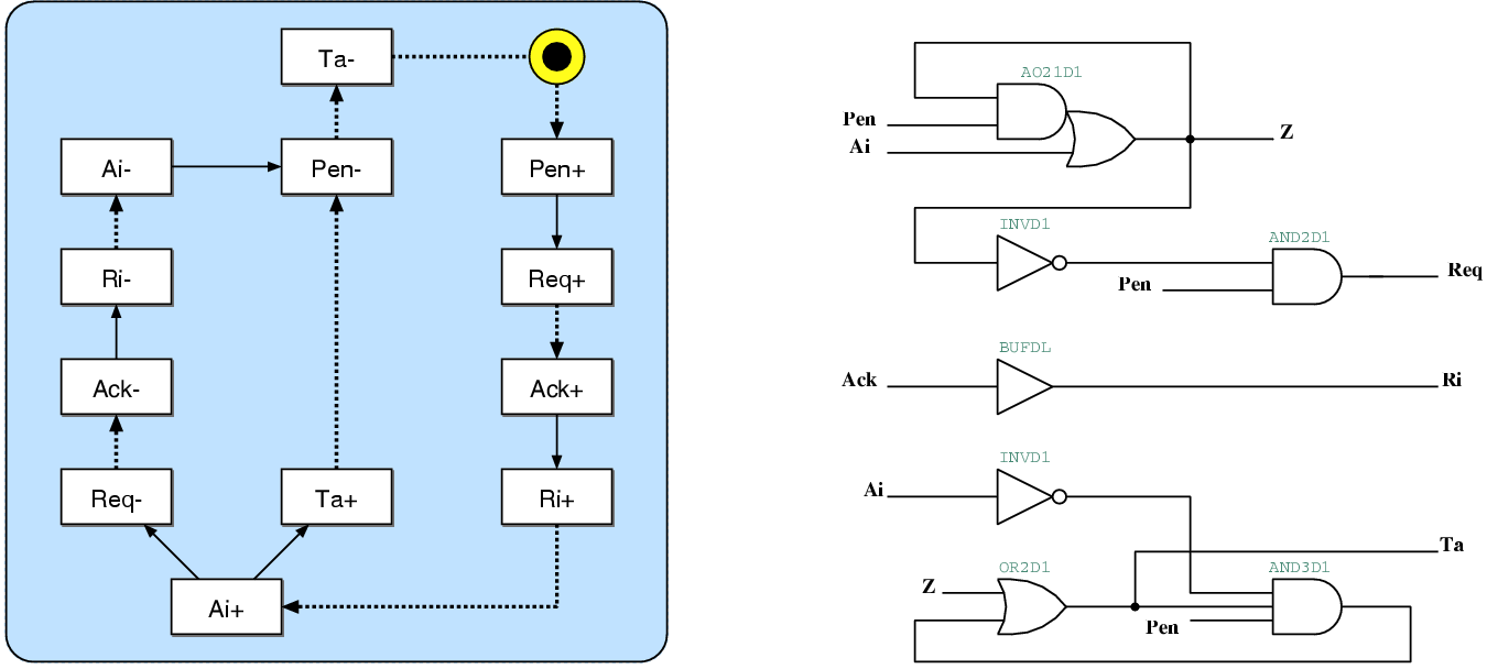
 Figure 5.4:
The state transition graph and the resulting
gate-level schematic of the d2g port controller. This port
is used for the communication between David and Goliath
on the David side.
The g2d port controller seen in figure 5.5
is very similar to the d2g. The Ri+ transition,
that will instruct the local clock generator to pause the clock, can
only fire after both Pen+ (coming from d2g)
and Req+ (coming from Goliath) are received.
At this point, David is ready to transfer data, the local clock
is paused immediately, and the Ack signal is generated.
Once the Req- signal is received, data transfer
has been completed and the local clock is released again. Similar
to d2g, the Ta signal is set immediately
after pausing the clock and remains active until Pen-
is received.
Figure 5.4:
The state transition graph and the resulting
gate-level schematic of the d2g port controller. This port
is used for the communication between David and Goliath
on the David side.
The g2d port controller seen in figure 5.5
is very similar to the d2g. The Ri+ transition,
that will instruct the local clock generator to pause the clock, can
only fire after both Pen+ (coming from d2g)
and Req+ (coming from Goliath) are received.
At this point, David is ready to transfer data, the local clock
is paused immediately, and the Ack signal is generated.
Once the Req- signal is received, data transfer
has been completed and the local clock is released again. Similar
to d2g, the Ta signal is set immediately
after pausing the clock and remains active until Pen-
is received.
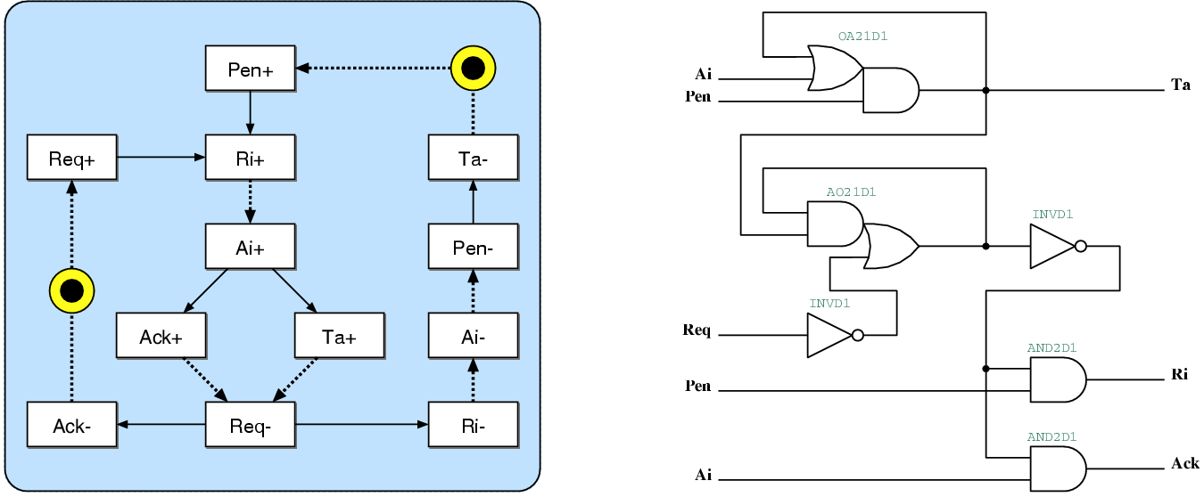
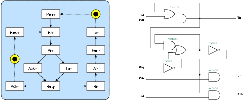 Figure 5.5:
The state transition graph and the resulting
gate-level schematic of the g2d port controller. This port
is used for the communication between David and Goliath
on the Goliath side.
Figure 5.5:
The state transition graph and the resulting
gate-level schematic of the g2d port controller. This port
is used for the communication between David and Goliath
on the Goliath side.
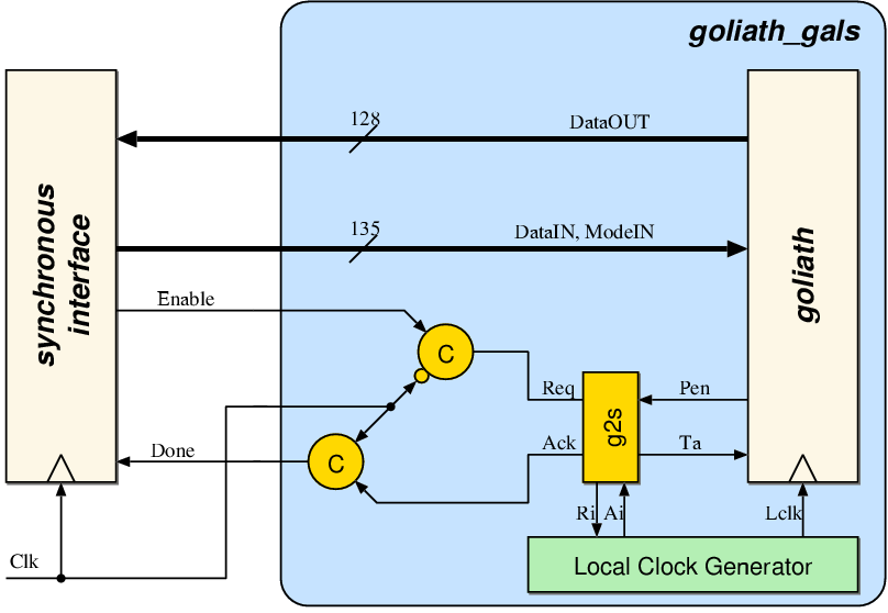
5.2.3 Data Exchange between Goliath and Synchronous Interface
The block diagram in figure 5.6
shows the data channel between Goliath and the synchronous
interface. This is a specialized interface as the synchronization
effort is only on the Goliath side of the channel. Note that,
in this organization, safe data transfers are only possible under
specific timing assumptions. In Acacia the external clock used
in the interface is chosen to be slower than the local clock generator
of Goliath. The port controller g2s ensures that Goliath
can synchronize within one clock period of the external clock signal.
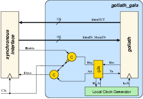 Figure 5.6:
The interface between
Goliath and the synchronous interface. The one-sided port g2s
is responsible for safe data transfers between two domains.
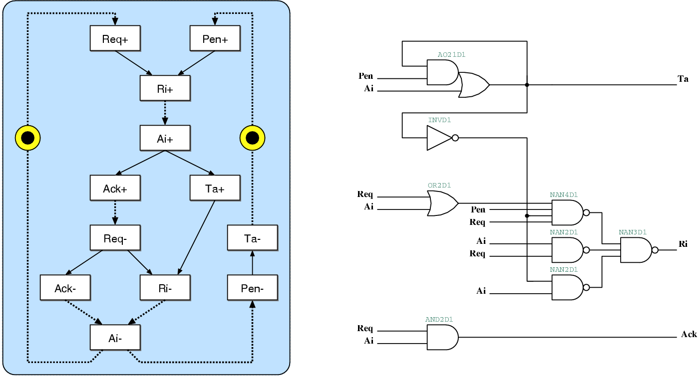
The STG and the gate-level circuit schematic for the port controller
g2s is given in figure 5.745. The Muller-C elements shown in figure 5.6
are used to change the handshake signals synchronous to the external
clock.
Figure 5.6:
The interface between
Goliath and the synchronous interface. The one-sided port g2s
is responsible for safe data transfers between two domains.
The STG and the gate-level circuit schematic for the port controller
g2s is given in figure 5.745. The Muller-C elements shown in figure 5.6
are used to change the handshake signals synchronous to the external
clock.
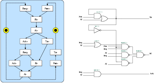 Figure 5.7:
The state transition graph and the resulting
gate-level schematic of the g2s port controller. This port
is used for the communication between Goliath and the synchronous
interface.
The synchronous interface initiates the data transfer by activating
the Enable signal, which is propagated to the Req
signal that triggers the g2s port. As soon as the port controller
is enabled by Goliath, Ri is activated to
pause the local clock. At this moment, it is safe to transfer data
between two modules and the Ack signal is activated.
The Muller-C element ensures that the Ack signal
generated by g2s is only propagated during the first half of
the clock period. In this way, the Done signal can
safely be sampled by the synchronous interface. The synchronous interface
then deactivates the Enable signal. The Muller-C
element allows Req to be deactivated within the
first half of the clock period only. The local clock of Goliath
remains paused until the arrival of the Req signal.
Contrary to the data transfers between David and Goliath,
there is no need to disguise the data transfers between Goliath
and the synchronous interface for DPA security.
No latches are required for the data transfer between the synchronous
interface and Goliath. The output registers of the synchronous
register are stable before the data transfer is initiated by the Enable
signal. The local clock of Goliath is paused as soon as it
starts the data transfer. The clock is paused until the Enable
signal is deactivated. This only happens after an active clock edge
on the synchronous interface. By this time the same clock edge will
safely sample the data inputs.
Figure 5.7:
The state transition graph and the resulting
gate-level schematic of the g2s port controller. This port
is used for the communication between Goliath and the synchronous
interface.
The synchronous interface initiates the data transfer by activating
the Enable signal, which is propagated to the Req
signal that triggers the g2s port. As soon as the port controller
is enabled by Goliath, Ri is activated to
pause the local clock. At this moment, it is safe to transfer data
between two modules and the Ack signal is activated.
The Muller-C element ensures that the Ack signal
generated by g2s is only propagated during the first half of
the clock period. In this way, the Done signal can
safely be sampled by the synchronous interface. The synchronous interface
then deactivates the Enable signal. The Muller-C
element allows Req to be deactivated within the
first half of the clock period only. The local clock of Goliath
remains paused until the arrival of the Req signal.
Contrary to the data transfers between David and Goliath,
there is no need to disguise the data transfers between Goliath
and the synchronous interface for DPA security.
No latches are required for the data transfer between the synchronous
interface and Goliath. The output registers of the synchronous
register are stable before the data transfer is initiated by the Enable
signal. The local clock of Goliath is paused as soon as it
starts the data transfer. The clock is paused until the Enable
signal is deactivated. This only happens after an active clock edge
on the synchronous interface. By this time the same clock edge will
safely sample the data inputs.
5.3
Testing Acacia
As soon as a design using self-timed circuit techniques is mentioned,
the first question that pops up is:
"How are you going to test this circuit ?"
Self-timed circuits have always been regarded as being difficult to
test. A good overview of the self-timed testing problem is given in
a survey conducted by Hulgaard et al [HBB95]. There are
two main properties of self-timed circuits that make traditional testing
approaches infeasible:
- It is not possible to hold the state of a self-timed circuit using
a global signal.
In synchronous systems, once the clock is halted, the state of the
system is frozen. It can be observed and manipulated with ease. There
are well established methods (i.e. scan based testing) and proven
tools to support this approach. It is possible to support similar
functionality for self-timed circuits as well. But the required test
functionality must be part of the circuit definition from the beginning46.
- Self-timed circuits are (in principle) sensitive to all transitions
of their inputs.
This increases the amount of failure sources. In synchronous systems,
as long as all nodes have the correct value at the time of a clock
transition, the system will function correctly. Parasitic transitions
of intermediate nodes have no negative effect on functionality47 in a synchronous system. In self-timed circuits, such glitches can
have terminal consequences. Not only that, but signal transitions
that are faster or slower than normal may result in the circuit malfunctioning.
The problem is also exaggerated by the fact that there are many different
flavors of self-timed design methodologies, each with its own special
requirements.
Testing is an essential part of the IC manufacturing process. Since
there are very few self-timed circuits that have been manufactured
in the industry [Ron99], the quality of test solutions
for self-timed circuits, when compared to their synchronous counterparts,
is clearly lacking .
The self-timed test problem is tackled in two main directions:
- Using a functional approach
Certain faults in self-timed circuits lead to clearly observable behavior,
usually such circuits stop functioning altogether. Several approaches
have been proposed that rely mainly on such 'self-checking' behavior
[MH91,Wie95,
GVO+02].
- Modifying the self-timed circuit to support scan-based testing
Since scan based testing is well-known and effective, most self-timed
test methodologies try to add scan capability to state holding elements
[PF95,
KB95,
BPtB02]. Unfortunately, full-scan based
self-timed test methods incur a very large area penalty, at times
doubling the circuit area. In order to keep the overhead at acceptable
values, partial-scan methods have been suggested as well.
The GALS methodology developed by Muttersbach used a synchronous fall
back method, in which, for test purposes, all AFSMs were bypassed
and synchronous state machines were used instead. The resulting system
was a fully synchronous system that can be tested normally. This method
was more of an emergency solution and several alternatives were considered
that actually tested the AFSMs as well. The AFSMs used in the GALS
system are very limited in complexity. Therefore, instead of devising
a general method that is capable of testing any given AFSM, practical
methods that ensure adequate test coverage for the AFSMs used in the
GALS methodology were investigated
At first, a method that added scanable elements to the asynchronous
connections was considered. This method, similar to the one presented
in [BPtB02] introduces a very large area overhead. Such
an arrangement also interrupts the asynchronous handshake signals
between GALS modules, slowing the communication and reducing the throughput.
Since all AFSMs are tested in isolation, this method fails to detect
delay faults that occur because signal transitions between two AFSMs
are either too slow or too fast. On top of that, it was shown that
the stuck-at test coverage of this approach is not above 90%.
In a GALS system, only a very small portion of all stuck-at faults
are in the AFSMs. As an example, in Acacia, the total number
of stuck-at faults is 154,604. Only 182 (0.118%) of these faults
are within the AFSMs. This was the main motivation to develop a functional
approach to test the AFSMs within the GALS system. This approach [GVO+02]
adds a Test Extension Element (TEE) to the each GALS module. The TEE
is clocked by a synchronous test clock. During test mode, the TEE
is able to decouple the Pen signal from the LS island
and initiate data transfers on all self-timed connections. In this
way, all data connections within the GALS system can be tested individually.
This idea is very similar in principle to the IEEE P1500 standard
proposed for testing embedded cores [MZK+99]: Inter-module
communication is tested by initiating data transfers between modules.
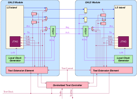 Figure 5.8:
Testing GALS systems with the
help of a test extension element. The self-timed wrapper includes
additional scan registers to insert and observe data transfer between
GALS modules. The centralized test controller can be realized on-chip,
or externally as a test program on automated test hardware
Individual TEEs are controlled by a centralized test controller as
seen in figure 5.8. The centralized
test controller could be implemented in hardware, giving the system
a built-in self-test capability, or implemented as a test program
on automated test equipment. The TEE also enables the test controller
to access the LS island through a JTAG interface. In this methodology,
all LS islands are assumed to have their own test solution.
Two GALS designs have been implemented after the test extension methodology
was developed. Shir-Khan [GOV03a] was designed primarily
as a test platform for various multi-point interconnection schemes
for GALS [Vil05]. Shir-Khan consists of twenty
five identical 4-bit micro-controllers with large buffers at their
inputs and outputs. These so-called port processors were specifically
designed to test the self-timed connections between the GALS modules.
A special local clock generator developed by Stephan Oetiker [OVG+02]
enabled switching between the locally generated clock and an external
synchronous clock for configuration. In a way, the functionality of
the TEE was integrated into the LS island and the local clock generator.
The local clock generator for Acacia uses a similar method
to switch between the locally generated clock and an external synchronous
test clock. During test mode, all GALS modules are run with the same
synchronous test clock. This allows standard tools to be applied to
generate the ATPG patterns. All LS islands are fully tested using
this method. However, the stuck-at faults within the AFSMs, the local
clock generators, and the data interface including the latches used
for retaining data, can not be detected with these patterns. Figure
5.9 shows the configuration that has
been used in Acacia. The shaded areas represent the portions
of the system that contain stuck-at faults that can not directly be
detected using the scan chains.
Figure 5.8:
Testing GALS systems with the
help of a test extension element. The self-timed wrapper includes
additional scan registers to insert and observe data transfer between
GALS modules. The centralized test controller can be realized on-chip,
or externally as a test program on automated test hardware
Individual TEEs are controlled by a centralized test controller as
seen in figure 5.8. The centralized
test controller could be implemented in hardware, giving the system
a built-in self-test capability, or implemented as a test program
on automated test equipment. The TEE also enables the test controller
to access the LS island through a JTAG interface. In this methodology,
all LS islands are assumed to have their own test solution.
Two GALS designs have been implemented after the test extension methodology
was developed. Shir-Khan [GOV03a] was designed primarily
as a test platform for various multi-point interconnection schemes
for GALS [Vil05]. Shir-Khan consists of twenty
five identical 4-bit micro-controllers with large buffers at their
inputs and outputs. These so-called port processors were specifically
designed to test the self-timed connections between the GALS modules.
A special local clock generator developed by Stephan Oetiker [OVG+02]
enabled switching between the locally generated clock and an external
synchronous clock for configuration. In a way, the functionality of
the TEE was integrated into the LS island and the local clock generator.
The local clock generator for Acacia uses a similar method
to switch between the locally generated clock and an external synchronous
test clock. During test mode, all GALS modules are run with the same
synchronous test clock. This allows standard tools to be applied to
generate the ATPG patterns. All LS islands are fully tested using
this method. However, the stuck-at faults within the AFSMs, the local
clock generators, and the data interface including the latches used
for retaining data, can not be detected with these patterns. Figure
5.9 shows the configuration that has
been used in Acacia. The shaded areas represent the portions
of the system that contain stuck-at faults that can not directly be
detected using the scan chains.
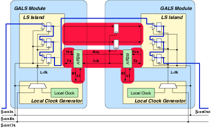 Figure 5.9:
Simplified schematic of the scan
chain connection used in Acacia. Once the ScanEn
signal is active, the GALS system is in test mode. All scan chains
of individual LS islands are connected and standard ATPG test vectors
can be used to test the circuit. The shaded areas represent the portions
of the circuit that is not covered by these tests. Functional test
vectors are used to detect the stuck-at faults in these areas.
The final gate-level netlist of Acacia was analyzed using Synopsys
Tetramax. All faults regarding the local clock generators48 and reset signals49 were removed from the fault library. The tool reported a test coverage
of 96.2%. A further analysis yielded the following:
Figure 5.9:
Simplified schematic of the scan
chain connection used in Acacia. Once the ScanEn
signal is active, the GALS system is in test mode. All scan chains
of individual LS islands are connected and standard ATPG test vectors
can be used to test the circuit. The shaded areas represent the portions
of the circuit that is not covered by these tests. Functional test
vectors are used to detect the stuck-at faults in these areas.
The final gate-level netlist of Acacia was analyzed using Synopsys
Tetramax. All faults regarding the local clock generators48 and reset signals49 were removed from the fault library. The tool reported a test coverage
of 96.2%. A further analysis yielded the following:
- 2,900 faults were classified as 'possibly detected'. Tetramax classifies
a fault as possibly detected if the fault simulation does not result
in a logic-1 or logic-0, but an unknown. By default, 50% credit is
given for such faults. Although this increases the test coverage by
few percentage points, these faults need to be investigated further
- 2,529 faults were listed as 'ATPG Undetectable'. Faults classified
as ATPG undetectable are tied to a constant value during the fault
simulation. Most of the faults in this class are a result of the test
mode signals that enable the circuit to be run synchronously.
- 351 faults were listed as 'Undetectable'. There are a number of reasons
why a fault can be placed in this class. Most common reasons are not
connected outputs or inputs that are tied to a constant value. Most
of these are plain design errors and could be eliminated during the
design phase. Tetramax automatically removes these faults from the
statistics.
- 1,897 faults were not detected.
After this analysis, all questionable faults were collected. Several
of the faults were equivalent. In addition, for some nodes both the
stuck-at-1 and stuck-at-0 faults could not be detected. A total of
3,089 unique nodes were determined by parsing the fault reports. A
gate-level simulation was performed and all of these 3,089 nodes were
observed for the duration of a simple encryption and decryption. Each
node that was observed to have changed its value more than 4 times
during this simulation was considered to be detectable for stuck-at-1
and stuck-at-050. This method reported 2,796 (90.5%) of the specially analyzed nodes
detectable for stuck-at faults. Once these nodes were mapped back
to the individual faults, only 175 faults remained undetected in the
entire design. This results in a respectable test coverage of 99.89%.
5.4 Adapting Modules for GALS
In principle, any standard synchronous design can be converted into
a GALS system. However, the advantages offered by the GALS methodology
can only be exploited if the system is designed with GALS in mind
from the beginning [GOK+05]. In a GALS system, the synchronous
design will be partitioned into several LS islands that will eventually
become individually clocked GALS modules. Each of these LS islands
have to be adapted to, or better yet designed according to, the requirements
of the GALS design. The better the synchronous system is adapted to
a GALS methodology, the better the performance will be. However, this
may result in a design that is noticeably different from a system
that is optimized for synchronous clocking.
As an example, consider the AES algorithm presented in this thesis.
An efficient synchronous design would most probably use a block diagram
like the one presented in figure 3.10. However, a
direct GALS implementation of this block diagram would not be able
to offer the same kind of DPA countermeasures as Acacia does.
Similarly, a designer would not come up with the transformation presented
in figure 4.1 without thinking about
a GALS implementation.
The following is a brief discussion of several key issues that must
be considered when designing GALS-friendly LS islands:
- Additional registers at inputs and outputs
The interface between the (locally) synchronous domain and the self-timed
domain is always prone to timing violations. The self-timed port controllers
ensure safe data transfers under the assumption that output data is
available when the port is activated and input data can be sampled
by the first active clock edge that follows the data transmission.
This can be achieved by using registers at both inputs and outputs.
Note that these registers are not strictly necessary for correct operation,
but they eliminate the costly timing verification effort at the interface.
The obvious side effect of this approach is additional latency in
the LS island. However, this additional latency is in local clock
cycles and may not translate to an overall latency in the system.
By isolating LS islands from the rest of the system, it may be possible
to run individual LS islands at a higher rate than what it would be
possible in a synchronous system. As an example in Acacia,
David can be clocked much faster than Goliath as can
be seen in table 4.3. As a net result, although
the GALS implementation requires 30% more clock cycles, the time
required to complete an AES round does not change significantly.
- Limited interaction between modules
Basically each data transfer between GALS modules has a chance to
slow the participating modules down. Therefore, a successful GALS
partitioning aims to limit the rate of data transfers between GALS
modules as much as possible. This requires fairly independent modules
that can operate on a set of data over several clock cycles before
requiring data exchange.
In synchronous systems, the actual state of a module can be easily
communicated across the system by several status bits. This can be
used to improve performance in the synchronous system. Communicating
such signals between GALS modules can be costly and should be avoided.
Again taking Acacia as an example: David requires several
cycles to process its input. Once David is finished, Goliath
needs to make a decision as to what to do next. In the synchronous
reference realization of Acacia the current state of Matthias
can be made available to Schoggi at all times. This enables
the decision process in Schoggi to be triggered as soon as
Matthias starts processing the last step. By the time Matthias
is finished, Schoggi has already reached a decision. In the
GALS implementation, communicating the actual state of David
to Goliath would require continuous data transfer between the
modules and is therefore not very practical.
The LS islands of a GALS system must be designed to operate using
one-time or burst-type parallel data/control signal transfers rather
than a continuous interaction. This may require re-engineering of
several control structures and result in performance loss in local
clock cycles.
- Proper handshake signals
There are various forms of handshake protocols that are available
to designers. However, a significant part of designers that are used
to synchronous systems do not apply them properly. Many designs use
protocols that are not complete and make a lot of (hidden) assumptions
on the system. Strobe signals are a good example for this. A strobe
signal basically qualifies an accompanying data signal as valid during
a clock cycle. This is equivalent to a request signal used in standard
handshake protocols. Such a signal assumes that the system is ready
to accept data at any clock cycle. Whether or not the data has been
accepted by the receiver is never really checked.
The LS islands of a GALS system needs to support proper handshaking
between the LS island and the port controllers. The exact handshake
protocol depends on the design of the specific port controllers used
in the system.
- More complex state machines
A GALS system consists of multiple GALS modules, each of which uses
its own local clock. When seen from a LS island that is part of a
GALS system, a data transaction to a connected GALS module may take
an undetermined amount of clock cycles. LS islands that have connections
to more than one GALS module are at times unable to make any assumptions
on the completion order of the data transactions.
Consider the controller in Goliath that schedules 32-bit operations
on two separate David units. Assume that initially both David
modules, David Perels and David Tschopp, are able to
accept data. Goliath will now wait for the modules to finish
processing, and schedule new operations on both units. At any given
clock cycle, both, any, or none of the two David modules may
return a result. Again, assume for a moment that David Perels
has returned a result and was assigned a third 32-bit data. Even now,
it is still possible that David Perels returns a result prior
to David Tschopp51.
Although it is very difficult to quantify, a controller within a GALS
module needs to consider more cases than a purely synchronous design,
and as a result is more complex.
- Reducing clock domains
One of the main challenges in modern SoC design is to handle a multitude
of clock domains. This requires considerable effort in synchronization,
and more often than not results in large FIFO structures between blocks.
Most of the clock domains are introduced to the system in order to
support a specific standard communication protocol. Different clock
domains are also used when parts of the SoC can not match certain
clock rates that are used throughout the system.
GALS is a method for synchronizing different clock domains. Although
it might sound strange, the goal of a GALS design must be to reduce
the number of clock domains. Each LS island will eventually be a separate
clock domain, and GALS provides a method to synchronize these domains.
If the synchronous system includes several clock domains, the GALS
system will have to be designed in a way to encapsulate each clock
domain in a separate GALS module. This may severely restrict the partitioning
and result in sub-optimum designs.
The data connection between two GALS modules can, in a way, be considered
as a single-stage distributed FIFO. At least theoretically, additional
FIFO buffers between individual modules should be unnecessary.
For an efficient SoC implementation, most of the tricks that were
added to the system in hope of supporting a synchronous design flow
need to be undone first. This may require at times radical changes
to the system.
- Real-time processing
Since GALS modules use a pausable local clock, it is very difficult
to guarantee that a certain operation can be processed in a fixed
number of clock cycles. At first sight, this makes it difficult to
interface external signals that have fixed clock rate.
However, most external interfaces use a decidedly slower clock rate
when compared to internal clock rates. Depending on the clock rates
used, it may still be possible to design interface modules that can
finish processing input and output in time for a fixed interface clock.
These interfaces have additional timing constraints set on them, and
especially with modules that have more than one connection, the conditions
to guarantee safe operation is not well defined.
Acacia uses such a port controller to communicate with a fixed-clock
interface. The particular interface described in section 4.3.3
uses a handshake protocol and does not expect results in a fixed number
of clock cycles. As long as the throughput requirement can be met
by the GALS modules, it would have been possible to meet fixed clock
cycle demands as well.
5.5 Related Research Directions
This thesis primarily presented an application of GALS to secure cryptographic
hardware design. There are other interesting fields where GALS could
have a potential impact. The following is a short description of three
active research fields where GALS could be used.
5.5.1 Network-on-Chip Systems
As SoCs grow in size, supporting a global communication that connects
all sub-modules becomes an increasingly difficult task. A solution
to this problem might be adapting network solutions commonly used
for computer communications within the SoC. Such systems are generally
referred to as Network-on-Chip (NoC) [JT03].
A classical NoC system, consists of several resources, which are regular
users of the network. Each resource is connected to the network by
a switch that is able to route data packets to and from the resource.
The NoC system clearly separates function from communication. The
functionality is provided by the resources, and the communication
between resources is handled by the switches.
Most of the topologies presented in the literature make use of the
two dimensional structure of an integrated circuit. Some architectures
like Nostrum [MNT+04] use a homogeneous mesh-based system,
while others like Xpipes [BB04] use a heterogeneous approach
where the geometry and size of resources is determined by the functionality.
The problem is very similar to the partitioning problem presented
for GALS systems in section 4.1. It is easier
to resolve the timing issues for homogeneous systems since all connections
between switches will have approximately the same size, on the other
hand it is difficult to imagine practical systems where all resources
are of identical size.
NoC solves one important problem of large system designs. Instead
of using overly long interconnections between sub-modules, data transmission
over longer distances is routed over switches in the network. Still
the problem of distributing a global clock to the entire system, and
synchronizing between different clock domains remains to be a challenge.
There are many parallels between NoC system design and GALS design.
First of all, both methods separate function from communication. As
mentioned earlier, the partitioning problem is very similar for both
approaches. Furthermore, both methods were developed to address problems
of large SoC designs. Combining both methods could potentially be
mutually beneficial. In fact, there are several recent publications
that talk about GALS-based NoC architectures
[BCV+05,
RVFG05].
A successful GALS-based NoC should be able to manage implementing
the resource as the LS island and realizing the switch as part of
the self-timed wrapper of a single GALS module. The switch should
not interfere with the LS island, as long as there is no data transfer
between the network and the resource. Note that, while the resource
is not receiving or sending data, the switch still needs to be able
to route traffic to and from connected switches. Depending on the
NoC system, this might require a more complex switch. In case the
network switch can not be realized easily using a self-timed design
method, it might be necessary to implement the switch as a second
LS island with an independent local clock generator, which would increase
the overhead of the system.
GALS would definitely address the problems of distributing the clock
and synchronizing between different clock domains. However, one of
the most requested features from a NoC system is a way to provide
Quality-of-Service (QoS). This guarantees a specific bandwidth between
selected resources under all circumstances. On the positive side,
the operation speed of the switches in a GALS-based NoC can be made
independent from the resource, adding more throughput and thus more
flexibility to the network. However, defining an upper limit for the
time that is required to transfer data between two GALS modules is
difficult52.
Overall, GALS and NoC promise to be two very compatible technologies.
Combining both could potentially help overcome several serious problems
that both technologies are facing at the moment.
5.5.2 Dynamic Voltage and Frequency Scaling
The more tightly circuits can be integrated, the more energy has to
be dissipated over the same area. Coupled with the demands of mobile
applications, where the power supply is one of the limiting design
parameters, this has strongly motivated the designers to find ways
to reduce the power consumption of integrated circuits over the last
years.
As outlined briefly in section 3.5.2,
the power consumption of an IC has a dynamic and a static part. While
decreasing technology size has increased the ratio of static power
consumption significantly, most of the power consumed by the integrated
circuits remains to be dynamic power consumption53 given by the following well-known equation:
The total switched capacitance C is determined mainly by the circuit
netlist, and the activity factor a is determined by the function
and input data. Even if the circuit is not changed in any way (and
C and a remain constant), the dynamic power consumption
can be reduced by both the operating frequency f and the supply
voltage Vdd.
The throughput of the circuit is directly determined by the operating
frequency, and reducing f will reduce the throughput of the circuit.
There are however some synchronous designs where the operating frequency
is chosen as a compromise to satisfy different requirements of the
circuit. In this case, some sub-blocks of the circuit may remain idle
over several clock cycles. Similarly, the throughput requirement of
the circuit may change throughout the operation of the circuit. Peak
throughput might only be required for short time intervals.
Reducing the supply voltage reduces the dynamic power consumption
even more decidedly. However, the power supply can not be reduced
indefinitely, and the circuits will slow down as the supply voltage
is reduced [CSB92].
Dynamically changing the frequency and the supply voltage for sub-blocks
to reduce power consumption has been successfully implemented for
high-performance micro-processors[NCM+02]. The so-called Dynamic
Voltage and Frequency Scaling (DVFS) methods are very attractive for
the micro-processors, as they are well-known for their excessive power
consumption, and their performance requirements strongly depend on
the program they are executing. Most DVFS applications are rather
coarse grained and adjustments are made after thousands or even millions
of clock cycles.
There is no reason why not also large SoC systems could benefit from
DVFS. There are some important differences between two design styles.
Unlike micro-processors, that have a relatively fixed architecture,
SoC architectures are more varied. Consequently, algorithms that are
developed to control DVFS for micro-processors are not always well
suited for SoC designs.
GALS offers several interesting advantages that could be exploited
to realize DVFS systems. The GALS design methodology already enables
modules to be clocked at different clock rates. At least theoretically,
it would be possible to extend this idea to support different voltages
as well. One important issue in DVFS is monitoring or predicting the
activity of the module to be controlled. In a GALS system that uses
D-type port controllers which pause the clock until data transfer
is completed, both the Req-Ack signal pairs or the
duty cycle of the local clock can be used to determine how active
a module is. If the duty cycle is
- 50%
- the module is running without being interrupted by data
transfers. This means that the environment is faster than (or at least
as fast as) the module itself. Potentially, the environment could
interact even with a faster module. Therefore, if it is possible,
increasing the operating frequency and the voltage of the module could
result in improved throughput.
- (50-d)%
- the module is running just as fast as the environment.
This is the ideal operating condition. The d value is required,
as it shows that the environment is just keeping up with the module,
and the module has to be paused occasionally.
- 25%
- the module is spending half the time waiting for the environment.
The module is producing results too fast. The supply voltage of the
module and the operating frequency of the local clock can be reduced
to save energy.
An important problem that needs to be addressed is to avoid cyclic
dependencies, where in the end all modules in a GALS system end up
slowing each other down until there is no activity at all. Also, instead
of relying solely on the environment to speed up operation, individual
GALS modules could be "warned" in advance about changes in activity54. These problems could be addressed by designing a centralized power
controller to monitor and control the DVFS effort in the GALS system.
A second problem is communication between modules with different power
supplies. Special level converters, or independent power supplies
for input and output registers could be used for this purpose. Unfortunately,
modern technologies have dramatically reduced power supplies to allow
small transistors. This reduces the available margin to adjust the
power supply of the module somewhat 55.
There is fair amount of interest and research already taking place
in adapting DVFS for GALS. However, published results are far away
from practical realizations. There are early theoretical studies on
the performance gains of GALS-based micro-processors using DVFS [IM02].
More recently published papers on GALS, like the GALDS approach by
Chattopadhyay et al. [CZ05], mention DVFS as a possible
application without providing concrete solutions.
5.5.3 Latency-Insensitive Design
Latency-insensitive circuits developed by Carloni et al. [CMSV01]
formally addresses the problem of designing systems whose inputs may
arrive with different latencies due to interconnection delays. Rather
than trying to find methods where all inputs arrive at the same time,
Carloni suggests adding relay stations on long interconnections. The
question is:
"Is it possible to have a functionally equivalent circuit under
these circumstances ?"
For the formal description of the system, a tagged signal model is
used. In this model, all signals are represented by a set of value-tag
pairs. The tag is essentially a timestamp that tells when the signal
has the given value. Using this notation, Carloni was able to prove
that, as long as the system consists of patient processes, it is indeed
possible to have a functionally equivalent system. Such systems are
called latency insensitive. A patient process is described as a stallable
process which can be halted until all data inputs required to generate
the next output are present.
Latency insensitive design was developed with synchronous systems
in mind. Most of the publications in this field try to address practical
issues on how relay stations can be added to the system. Functional
blocks are encapsulated by a shell that converts the system into a
patient system, mostly by adequate clock gating. This approach is
remarkably similar to a GALS system that consists of functional LS
islands encapsulated by a self-timed wrapper, which contains a pausable
local clock. The analysis methods used in latency-insensitive design
may be applied to GALS systems and can be used to address formal aspects
of GALS system design.
File translated from
TEX
by
TTH,
version 3.77.
On 20 Dec 2006, 15:44.